Download
1 / 42
430 likes | 536 Views
Explore semiconductors' crystal structures, bonding, and band structures in Group IV and Group III-V compounds. Learn about the covalent and ionic components in these materials. Discover the characteristics of semiconductors and their potential applications in electronic devices.

E N D
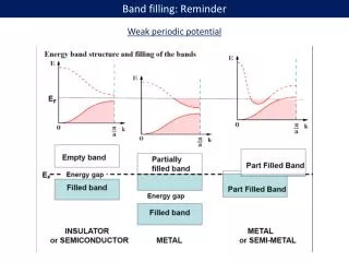
Band filling: Reminder Weak periodic potential
Semiconductors Crystal structure and bonding Semiconductors include a large number of substances of widely different chemical and physical properties. These materials are grouped into several classes of similar behavior, the classification being based on the position in the periodic table of the elements. The best-known class is the Group IV semiconductors (now it is denoted as Group 14) C (diamond), Si, Ge, all of which lie in the fourth (now 14th) column of the periodic table. They have been studied intensively, particularly Si and Ge, which have found many applications in electronic devices. The elemental semiconductors all crystallize in the diamond structure. The diamond structure has a fcc lattice with a basis composed of two identical atoms, and is such that each atom is surrounded by four neighboring atoms, forming a regular tetrahedron. Group IV semiconductors are covalent crystals, i.e., the atoms are held together by covalent bonds. These bonds consist of two electrons of opposite spins distributed along the line joining the two atoms. The covalent electrons forming the bonds are hybrid sp3 atomic orbitals.
Another important group of semiconductors is the Group III-V compounds, so named because each contains two elements, one from the third and the other from the fifth column of the periodic table (now the columns 13 and 15, respectively. The best-known members of this group are GaAs and InSb (indium antimonite), but the list also contains compounds such as GaP, InAs, GaSb, and many others. These substances crystallize in the zincblendstructure which is the same as the diamond structure, except that the two atoms forming the basis of the lattice are now different. Thus, in GaAs, the basis of the fcc lattice consists of two atoms, Ga and As. Because of this structure, each atom is surrounded by four others of the opposite kind, and these latter atoms form a regular tetrahedron, just as in the diamond structure. The bonding in the III-V compounds is also primarily covalent. The eight electrons required for the four tetrahedral covalent bonds are supplied by the two types of atoms, the trivalent atom contributing its three valence electrons, and the pentavalent atom five electrons.
13 15
However, the bonding in this group is not entirely covalent. Because the two elements in the compound are different, the distribution of the electrons along the bond is not symmetric, but is displaced toward one of the atoms. As a result, one of the atoms acquires a net electric charge. Such a bond is called heteropolar, in contrast to the purely covalent bond in the elemental semiconductors, which is calledhomopolar. The distribution of electrons in the bond is displaced toward the atom of higher electronegativity. In GaAs, for instance, the As atom has a higher electronegativity than the Ga, and consequently the As atom acquires a net negative charge, whose value is −0.46e per atom (a typical value in Group III-V compounds). The Ga atom correspondingly acquires a net positive charge of 0.46e. Charge transfer leads to an ionic contribution to the bonding in Group III-V compounds. Their bonding is therefore actually a mixture of covalent and ionic components, although covalent ones predominate in most of these substances.
Band structure An intrinsic semiconductor is a solid in which the highest occupied energy band, the valence band, is completely full at T = 0°K, but in which the gap above this band is also small, so that electrons may be excited thermally at room temperature from the valence band to the next-higher band, which is known as the conduction band. Generally speaking, the number of excited electrons is appreciable (at room temperature) whenever the energy gap Egis less than 2 eV. The substance may then be classified as a semiconductor. When the gap is larger, the number of electrons is negligible, and the substance is an insulator. When electrons are excited across the gap, the bottom of the conduction band (CB) is populated by electrons, and the top of the valence band (VB) by holes. As a result, both bands are now only partially full, and would carry a current if an electric field were applied. The conductivity of the semiconductor is small compared with the conductivities of metals of the small number of electrons and holes involved, but this conductivity is nonetheless sufficiently large for practical purposes. http://britneyspears.ac/lasers.htm
Manifestations of the band structure Light absorption
Since we are interested only in the region which lie close to the band gap, where electrons and holes lie, we can ignore a more complex variation of the energy bands far away from the gap. The energy of the CB has the form where k is the wave vector and methe effective mass of the electron. The energy Egrepresents the energy gap. The zero-energy level is chosen to lie at the top of the VB. The energy of the VB may be written as where mhis the effective mass of the hole which is positive. (Because of the inverted shape of the VB, the mass of an electron at the top of the VB is negative, but the mass of a hole is positive.) Within this simple picture of the semiconductor, the primary band-structure parameters are thus the electron and hole masses me andmh, and the band gapEg.
The energy gap in a semiconductor varies with temperature, but the variation is usually slight. That a variation with temperature should exist at all can be appreciated from the fact that the crystal, when it is heated, experiences a volume expansion, and hence a change in its lattice constant. This, in turn, affects the band structure, which is a sensitive function of the lattice constant. Band structures of real semiconductors are somewhat more complicated, as we shall see, but for the present the simplest structure will suffice for our purposes.
Effective mass approximation is valid only close to the extremes of the dispersion relations En(k). Far from these points the effective mass depends on k (non-parabolicity) – typical for metals, but may also be important for semiconductors. Even close to the band edges the dispersion relation can be anisotropic. In that case the inverse effective mass is a tensor.
Intrinsic Semiconductors In the field of semiconductors electrons and holes are usually referred to as free carriers, or simply carriers, because it is these particles which are responsible for carrying the electric current. The number of carriers is an important property of a semiconductor, as this determines its electrical conductivity. Intrinsic semiconductors are semiconductors in which the number of carries and the conductivity is not influenced by impurities. Intrinsic conductivity is typical at relatively high temperatures in highly purified specimens. In order to determine the number of carriers, we need to recall some of the basic results of statistical mechanics. The most important result in this regard is the Fermi-Dirac (FD) distribution function which is the probability that an energy level E is occupied by an electron when the system is at temperature T.
We will see later that the Fermi level in intrinsic semiconductors lies close to the middle of the band gap. Therefore we can represent the distribution function and the conduction and valence bands of the semiconductor as shown in the figure. Distribution function Density of states for electrons and holes Conduction and valence bands
The equation relating the concentration of the electron with the chemical potential reads: The band gap in semiconductors is of the order of 1eV, which is much larger than kBT. Therefore . Furthermore, in 3D As a result,
The concentration of holes is given by a similar expression: where As a result The neutrality condition, n=p, yields . Therefore The second term on the right is very small compared with the first, and the energy level is close to the middle of the energy gap. This is consistent with earlier assertions that both the bottom of the CB and the top of the VB are far from the Fermi level.
The concentration of electrons may now be evaluated explicitly as The important feature of this expression is that n increases very rapidly - exponentially - with temperature, particularly by virtue of the exponential factor. Ge Thus as the temperature is raised, a vastly greater number of electrons is excited across the gap. For Ge at room temperature n ~ 1014electrons/cm3, a typical value of carrier concentration in semiconductors. When the substance is impure, additional electrons or holes are provided by the impurities. In that case, the concentrations of electrons and holes may no longer be equal, and the amount of each depends on the concentration and type of impurity present. When the substance is sufficiently pure so that the concentrations of electrons and holes are equal, we speak of an intrinsic semiconductor. That is, the concentrations are determined by the intrinsic properties of the semiconductor itself. On the other hand, when a substance contains a large number of impurities which supply most of the carriers, it is referred to as an extrinsic semiconductor.
Impurity states A pure semiconductor has equal numbers of both types of carriers, electrons and holes. In most applications, however, one needs specimens which have one type of carrier only, and none of the other. By doping the semiconductor with appropriate impurities one can obtain samples which either electrons or holes only. Example: Si doped by As. The As atoms (the impurities) occupy some of the lattice sites formerly occupied by the Si host atoms. The distribution of the impurities is random throughout the sample. But their presence is important since the As atom has valence 5 while Si has valence 4. Of the 5 electrons of As, 4 participate in the tetrahedral bond of Si. The 5th electron cannot enter the bond, which is now saturated, and hence this electron detaches from the impurity and can migrate through the crystal as a conduction electron - it enters the CB. The impurity now actually a positive ion, As+ (since it has lost one of its electrons), and thus it tends to capture the free electron, but we shall show shortly that the attraction force is very weak, and not enough to capture the electron in most circumstances.
The net result – As impurities contribute electrons to the CB of the semiconductors, and for this reason these impurities are called donors. Note that the electrons have been created without the generation of holes. When an electron is captured by an ionized donor, it orbits around the donor much like the situation in hydrogen. We can calculate the binding energy by using the familiar Bohr model. However, we must take into account the fact that the Coulomb interaction here is weakened by the screening due to the presence of the semiconductor crystal, which serves as a medium in which both the donor and ion reside. Thus the Coulomb potential is now given by where ε is the reduced dielectric constant of the medium. The dielectric constant ε = 11.7 in Si, for example, shows a substantial decrease in the interaction force. It is this screening which is responsible for the small binding energy of the electron at the donor site. Using this potential in the Bohr model, we find the binding energy, corresponding to the ground state of the donor, to be Note that the effective mass mehas been used rather than the free mass m.
The binding energy of the hydrogen factor atom, which is equal to 13.6 eV. The binding energy of the donor is reduced by the factor 1/ε2, and also by the mass factor me /m, which is usually smaller than unity. Using the typical values ε ~ 10 and me/m ~ 0.1, we find that the binding energy of the donor is about 10-3 of the hydrogen energy, i.e., about 0.01 eV. This is indeed the order of the observed values. It is instructive to evaluate the Bohr radius of the donor electron. Straightforward adaptation of the Bohr result leads to where a0 is the Bohr radius, equal to 0.53 Å. The radius of the orbit is thus much larger than a0, by a factor of 100, if we use the previous values for ε and me. A typical radius is thus of the order of 50 Å. Since this is much greater than the interatomic spacing, the orbit of the electron encloses a great many host atoms, and our picture of the lattice acting as a continuous, polarizable dielectric is thus a plausible one.
Since the donors are almost all ionized, the concentration of electrons is nearly equal to that of the donors. Typical concentrations are about 1015 cm-3. But sometimes much higher concentrations are obtained by heavy doping of the sample, for example, 1018 cm-3 or even more. Acceptors An appropriate choice of impurity may produce holes instead of electrons. Suppose that the Si crystal is doped with Ga impurity atoms. The Ga impurity resides at a site previously occupied by a Si atom, but since Ga is trivalent, one of the electron bonds remains vacant . This vacancy may be filled by an electron moving in from another bond, resulting in a vacancy (or hole) at this latter bond. The hole is then free to migrate throughout the crystal. In this manner, by introducing a large number of trivalent impurities, one creates an appreciable concentration of holes, which lack electrons
The trivalent impurity is called an acceptor, because it accepts an electron to complete its tetrahedral bond. The acceptor is negatively charged, by virtue of the additional electron it has entrapped. Since the resulting hole has a positive charge, it is attracted by the acceptor. We can evaluate the binding energy of the hole at the acceptor in the same manner followed above in the case of the donor. Again this energy is very small, of the order of 0.01 eV. Thus essentially all the acceptors are ionized at room temperature. The acceptor level lies in the energy gap, slightly above the edge of the VB. This level corresponds to the hole being captured by the acceptor. When an acceptor is ionized (an electron excited from the top of VB to fill this hole) the hole falls to the top of the VB, and is now a free carrier. Thus the ionization process, indicated by upward transition of the electron on the energy scale, may be represented by a downward transition of the hole on this scale.
Semiconductor statistics Semiconductors usually contain both donors and acceptors. Electrons in the CB can be created either by thermal excitation or by thermal ionization of the donors. Holes in the VB may be generated by interband excitation, or by thermal excitation of electrons from the VB into the acceptor level. And in addition, electrons may fall from the donor levels to the acceptor level. Finding the concentrations of carriers, both electrons and holes, taking all these processes into account, is quite complicated. We shall treat a few special cases, which are often encountered in practice. Two regions may be distinguished, depending on the physical parameters involved: The intrinsic and the extrinsic regions.
The intrinsic region The concentration of carriers in the intrinsic region is determined primarily by thermally induced interband transitions. In this region n=p. The intrinsic region obtains when the impurity doping is small. When we denote the concentrations of donors and acceptors by Ndand Na, the requirement for the validity of the intrinsic condition is n >> Nd,Na. Since n increases rapidly with temperature, the intrinsic condition becomes more favorable at higher temperatures. All semiconductors, in fact, become intrinsic at sufficiently high temperatures (unless the doping is unusually high). The extrinsic region Quite often the intrinsic condition is not satisfied. For the common levels of doping encountered, about 1015 cm-3, the number of carriers supplied by the impurities is large enough to change the intrinsic concentration appreciably at room temperature. The contribution of impurities, in fact, frequently exceeds those carriers that are supplied by interband excitation. When this is so, the sample is in the extrinsic region. Two different types of extrinsic regions may be distinguished. The first occurs when the donor concentration greatly exceeds the acceptor concentration, that is, when Nd>> Na. In this case, the concentration of electrons may be evaluated quite readily.
Since the donor's ionization energy (i.e. the binding energy) is quite small, all the donors are essentially ionized, their electrons going into the CB. Therefore, to a good approximation, n=Nd. A semiconductor in which n >> p is called an n-type semiconductor (n for negative). Such a sample is characterized, as we have seen, by a great concentration of electrons. The other type of extrinsic region occurs when Na >> Nd, that is, the doping is primarily by acceptors. Using an argument similar to the above, one then has p=Na. i.e., all the acceptors are ionized. Such a material is called a p-type semiconductor. It is characterized by a preponderance of holes.
In discussing ionization of donors (and acceptors), we assumed that the temperature is sufficiently high so that all of these are ionized. This is certainly true at room temperature. But if the temperature is progressively lowered, a point is reached at which the thermal energy becomes too small to cause electron excitation. In that case, the electrons fall from the CB into the donor level, and the conductivity of the sample diminishes dramatically. This is referred to as freeze-out, in that the electrons are now "frozen" at their impurity sites.The temperature at which freeze-out takes place is Ed ~ kBT, which gives a temperature of about100° K.
Electrical conductivity; Mobility Electrical conductivity is, of course, the quantity of primary interest in semiconductors. Both the electrons and holes contribute to electric current. Assume first that a sample is strongly n-type and contains only one type of carrier: electrons. The conductivity can be treated according to the free electron model: To estimate the value for σe, we substitute n = 1014 cm-3, which is eight orders in magnitude less than that in metals, and me = 0.1 m. This leads to σe = 10-7 (μOhm⋅cm)-1 , which is a typical figure in semiconductors. Although this is many orders of magnitude smaller than the value in a typical metal, σe = 1 (μOhm⋅cm)-1,the conductivity in a semiconductor is still sufficiently large for practical applications. Semiconductor physicists often use another transport coefficient: mobility. The mobility μe is defined as the proportionality coefficient between the electron drift velocity and the applied electric field, ve= μeE
As defined, the mobility is a measure of the rapidity of the motion of the electron in the field. The longer the lifetime of the electron and the smaller its mass, the higher the mobility. We can now express electrical conductivity in terms of mobility as . Typical value for μemay be obtained by substituting σe=10-7 (μOhm⋅cm)-1 and n= 1014 cm-3 . This yields What we have said about electrons in a strongly n-type substance can be carried over to a discussion of holes in a strongly p-type substance. The conductivity of the holes is given by where μhis the hole mobility.
Let us now treat t he general case, in which both electrons and holes are present. When a field is applied, electrons drift opposite to the field and holes drift in the same direction as the field. The currents of the two carriers are additive, however, and consequently the conductivities are also. Therefore When the substance is in the intrinsic region, n = p, one has Dependence on temperature Conductivity depends on temperature, and this dependence is often pronounced. Consider a semiconductor in the intrinsic region. But in this situation the concentration n increases exponentially with temperature. We can write the conductivity as where F(T) is a function which depends only weakly on the temperature. Thus conductivity increases exponentially with temperature.
This result can be used to determine the energy gaps in semiconductors. In the early days of semiconductors this was the standard procedure for finding the energy gap. Nowadays, however, the gap is often measured by optical methods When the substance is not in the intrinsic region, the temperature dependence of the conductivity is not usually as strong as indicated above. To see the reason for this, suppose that the substance is extrinsic and strongly n-type. The conductivity is σ = neμe, but the electron concentration n is now a constant equal to Nd, the donor (hole) concentration. And any temperature dependence present must be due to the mobility of electrons or holes. Mobility versus temperature: scattering mechanisms Mobility of electrons (or holes) varies with temperature. In n-type semiconductor Since the lifetime of the electron, or its collision time, varies with temperature, its mobility also varies with temperature. Normally, both lifetime and mobility diminish as the temperature rises.
The relaxation time is given by where le is the electron mean free path, while ve is the average electron velocity. The velocity of electrons is different depending on their location in the conduction band. Electrons at the bottom of the conduction band in a semiconductor obey the classical statistics rather then the highly degenerate Fermi statistics prevailing in metals. The higher electrons are in the band the greater is their velocity. We can evaluate the conductivity by assuming that veis the average velocity. The average velocity can be estimated using the procedure of the kinetic theory of gases: This introduces a factor of T-1/2 dependence in the mobility:
leis determined by the various collision mechanisms acting on the electrons. These mechanisms are the collisions of electrons with thermally excited phonons and collisions with impurities. At high temperatures, at which collisions with phonons is the dominant factor, le is inversely proportional to temperature, that is, le~ T-1. In that case, mobility varies as μe ~ T-3/2. Another scattering mechanism in semiconductors is that of ionized impurities. When a substance is doped, the donors (or acceptors) lose their electrons (or holes) to the conduction band. The impurities are thus ionized, and are quite effective in scattering the electrons (holes). At high temperatures this scattering is masked by the phonon mechanism, but at low temperatures this latter mechanism becomes weak and the ionized-impurity scattering gradually takes over.
Band structure of real semiconductors So far, we have assumed the simplest possible band structure, namely, a conduction band of a standard one uses the actual band structure is bit possible to obtain a quantitative agreement form, centered at the origin, k = 0, and a valence band of a standard inverted form, also entered at the origin. Such a simple structure is applicable for elucidating many observed phenomena, but it does not represent the actual band structures of many common semiconductors. Only when one uses the actual band structure it is possible to obtain a quantitative agreement between experiments and theoretical analysis. GaAs Example:GaAS – the conduction band has a minimum at the origin k = 0, and the region close to the origin is well represented by a quadratic energy dependence with me = 0.072 m. As k increases, the energy E(k) is no longer quadratic in k, and those states may no longer by represented by a single, unique effective mass.
The next-higher energy minimum occurs along the [100] direction. The dependence of energy on k in the neighborhood of this secondary minimum is quadratic, and hence an effective mass may be defined but its value is much greater than that of the primary minimum (at the center). . The actual value is 0.36 m. GaAs Due to cubic symmetry there are six equivalent secondary minima, or valleys. These secondary valleys do not play important role under most circumstances, since the electrons usually occupy only the central valley. There are also other secondary valleys in the [111] directions. These are higher than the [100] valleys, and hence are even less likely to be populated by electrons. The valence band is also illustrated is composed of three closely spaced subbands. Because the curvatures of the bands are different, so are the effective masses of the corresponding holes. One speaks of light holes and heavy holes. III-V semiconductors have band structures quite similar to that of GaAs.
Band structure of Si. The conduction band has its lowest minimum not at k=0. The minimum lies along the [100] direction, at about 0.85 distance from the center to the edge of the zone. Note that the bottom of the conduction does not e directly above the top of the valence band. This type of semiconductors is known as indirect gap semiconductors. Because of the cubic symmetry there are actually six equivalent primary valleys located along the [100] directions. The energy surfaces at these valleys are composed of elongated ellipsoids of revolution whose axes of symmetry are along the [100] directions. There are two different effective masses which correspond to these surfaces The longitudinal mass is ml = 0.97m, while the identical transverse masses are mt = 0.19m. The mass anisotropy ratio is about 5.
The valence band in silicon is represented by three different holes. One of the holes is heavy (mh = 0.5m), and the other two are light. The energy gap in Si, from the top of the valence and to the bottom of the conduction band, is equal to 1.08 eV. The fact that the bottom of the conduction does not lie directly above the top of the valence band, is irrelevant to the definition of the band gap. Excitons An electron and a hole may be bound together by their attractive Coulomb interaction, just as an electron is bound to a proton to form a neutral hydrogen atom. The bound electron-hole pair is called an exciton. An exciton can move through the crystal and transport energy; it does not transport charge because it is electrically neutral. It is similar to positronium, which is formed from an electron and a positron. Excitons can be formed in every insulating crystal. All excitons are unstable with respect to the ultimate recombination process in which the electron drops into the hole.
The binding energy of the exciton can be measured by optical transitions from the valence band, by the difference between the energy required to create electron and free hole and the energy to create a free an exciton. Estimate of the binding energy. Consider an electron in the conduction band and a hole in the valence band. The electron and hole attract each other by the Coulomb potential There will be bound states of the exciton system having total energies lower than the bottom of the conduction band. The problem is the hydrogen atom problem if the energy surfaces for the electron and hole are spherical and non- degenerate. The energy levels are given by The ground state corresponds to n = 1 ; this is the ionization energy of the exciton.
Thermoelectric effects Consider a semiconductor maintained at a constant temperature while an electric field drives through it an electric current density jq. If the current is carried only by electrons, the charge flux is jq=enμe E The average energy transported by an electron is referred to the Fermi level μ, Ec- μ + (3/2) kBT where E, is the energy at the conduction band edge. We refer the energy to the Fermi level because different conductors in contact have the same Fermi level. The energy flux that accompanies the charge flux is jU=- nμe [Ec- μ + (3/2) kBT ] E . The Peltier coefficient is defined by jU = Πjq; or the energy carried per unit charge. For electrons Π=- [Ec- μ + (3/2) kBT ] and is negative because the energy flux is opposite to the charge flux for holes jq=epμh E, jU= pμh [μ - Ev + (3/2) kBT ] E and is positive
The absolute thermoelectric power Q is defined from the open circuit electric field created by a temperature gradient: E = Q grad T . The Peltier coefficient II is related to the thermoelectric power Q by Π= QT. This is the famous Kelvin relation of irreversible thermodynamics. A measurement of the sign of the voltage across a semiconductor specimen, one end of which is heated, is a rough and ready way to tell if the specimen is n type or p type. Peltier coefficient of n and p silicon as a function of temperature. Above 600 K the specimens act as intrinsic semiconductors. The curves are calculated and the points are experimental