
PHYSICS
E N D
Presentation Transcript
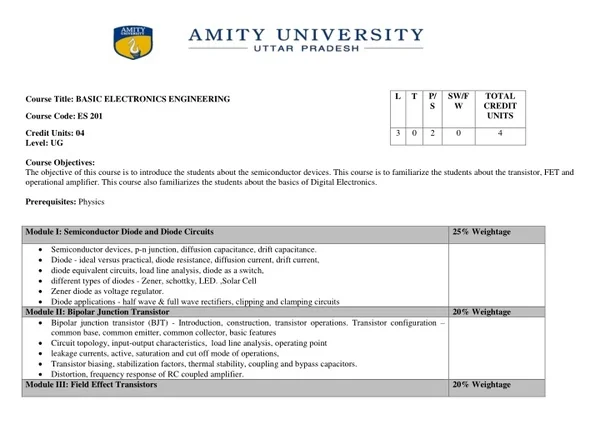
Course Title: BASIC ELECTRONICS ENGINEERING P/ S SW/F W TOTAL CREDIT UNITS L T Course Code:ES 201 Credit Units: 04 Level: UG Course Objectives: The objective of this course is to introduce the students about the semiconductor devices. This course is to familiarize the students about the transistor, FET and operational amplifier. This course also familiarizes the students about the basics of Digital Electronics. Prerequisites: Physics Module I: Semiconductor Diode and Diode Circuits 3 0 2 0 4 25% Weightage Semiconductor devices, p-n junction, diffusion capacitance, drift capacitance. Diode - ideal versus practical, diode resistance, diffusion current, drift current, diode equivalent circuits, load line analysis, diode as a switch, different types of diodes - Zener, schottky, LED. ,Solar Cell Zener diode as voltage regulator. Diode applications - half wave & full wave rectifiers, clipping and clamping circuits Module II: Bipolar Junction Transistor Bipolar junction transistor (BJT) - Introduction, construction, transistor operations. Transistor configuration – common base, common emitter, common collector, basic features Circuit topology, input-output characteristics, load line analysis, operating point leakage currents, active, saturation and cut off mode of operations, Transistor biasing, stabilization factors, thermal stability, coupling and bypass capacitors. Distortion, frequency response of RC coupled amplifier. Module III: Field Effect Transistors 20% Weightage 20% Weightage
Junction Field effect transistor (JFET) - volt-ampere characteristics Merits and demerits of JFET MOSFET - enhancement and -depletion mode, Common source amplifier Source follower Module IV: Introduction to Operational Amplifiers 20% Weightage Differential amplifier configuration, CMRR Introduction to Op-Amp, schematic and block diagram, equivalent circuit Pin configuration of 741 Op-Amp, datasheet interpretation Characteristics of ideal Op-Amp, concept of virtual ground, slew rate, Op-Amp configuration – open loop and closed loop Inverting and non-inverting Amplifiers Module V: Basic Digital Electronics 15% Weightage Number systems and codes, Boolean algebra, basic logic gates and their truth tables, Implementation of Boolean function using universal gates NAND and NOR, K-maps upto 4 variable Adders and subtractor. Student Learning Outcomes: Identify and describe operation of semiconductor devices. Students are able to analyze where and how analog and digital components are used Design basic amplifier circuits using BJT Construct application based circuits using diode/BJT/logic gates Pedagogy for Course Delivery: The course would be covered under theory and laboratory. In addition to assigning small project–based learning, early exposure to hands-on design to enhance the motivation among the students. It incorporates designing of problems, analysis of solutions submitted by the students groups and how learning objectives were achieved. Continuous evaluation of the students would be covered under quiz, viva etc. List of Laboratory Experiment 1.To study and plot the characteristics of a junction diode. 1.To study Zener diode I-V characteristics. 2.To study diode based clipping and clamping circuits. 3.To study half wave, full wave and bridge rectifier with filters. 4.To study the input and output characteristics of a transistor in its various configurations (CE and CB). 5.To study and plot the characteristics of a JFET in its various configurations.
6.To study and plot the characteristics of a MOSFET in its various configurations. 7.To study the gain and plot the frequency response of a single stage transistor amplifier. 8.To study the op amp as an inverting and non- inverting amplifier. 9.To verify the truth tables of NOT, OR, AND, NOR, NAND, XOR, XNOR gates. Assessment/ Examination Scheme: Theory L/T (%) Lab/Practical (%) Total 75% 25% 100% Theory Assessment (L&T): Continuous Assessment/Internal Assessment End Term Examination Components (Drop down) S/V/Q HA Mid-Term Exam(CT) Attendance(A) Weightage (%) 10% 8% 7% 5% 70% CT: Class Test, HA: Home Assignment, S/V/Q: Seminar/Viva/Quiz, EE: End Semester Examination; A: Attendance Lab Assessment (P): End Term Examination Continuous Assessment/Internal Assessment Components (Drop down) PR LR A V Weightage (%) 5% 10% 10% 5% 70% A: Attendance, PR- Performance, LR – Lab Record, V – Viva. EE- External Exam,
Text & References: Robert L. Boylestad and Louis Nashelsky, “Electronic Devices and Circuit Theory”,8th Edition., PHI, 2002. Millman J. and Halkias .C., " Integrated Electronics ", 2nd Edition, Tata McGraw-Hill, 2001. Adel S. Sedra and K. C. Smith: Microelectronic Circuits, Fifth Edition, 2007, ISBN-10: 0195338839. Ramakant Gaekwad: Operational Amplifiers and Linear Integrated Circuits fourth Edition, 2000, ISBN 0132808684, 9780132808682 Moris Mano: Digital Design, Pearson Education. FIFTH EDITIONISBN-13: 978-0-13-277420-8 , ISBN-10: 0-13-277420-8 Principles of digital design, Prentice-Hall, Inc. Upper Saddle River, NJ, USA ©1996 ,ISBN:0-13-301144-5