Download
1 / 12
180 likes | 605 Views
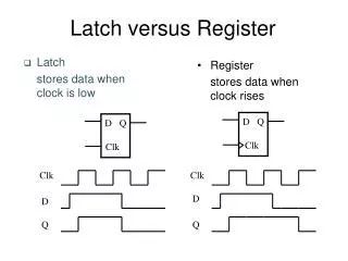
Latch-based Design. D. Q. Clk. T. Clk. t hold. D. t su. t c-q. Q. Register Parameters. Delays can be different for rising and falling data transitions. D. Q. Clk. T. Clk. PW m. t su. D. t hold. t d-q. t c-q. Q. Latch Parameters.

E N D
D Q Clk T Clk thold D tsu tc-q Q Register Parameters Delays can be different for rising and falling data transitions
D Q Clk T Clk PWm tsu D thold td-q tc-q Q Latch Parameters Delays can be different for rising and falling data transitions
tD-Q D Q Clk tClk-Q Latch timing • When data arrives to transparent latch • - latch is a “soft” barrier • When data arrives to closed latch • - data has to be ‘re-launched’
Flip-Flop – Based Timing Skew Flip-flop delay Logic delay f TSU TClk-Q Flip-flop f = 1 f = 0 Logic Representation after M. Horowitz, VLSI Circuits 1996.
Timing Constraints Basic constraints without clock skew and jitter Minimum cycle time: Tclk tc-q + tsu + tlogic Hold time constraint: t(c-q, cd) + t(logic, cd) thold
Latch-Based Timing Skew Static logic f L2 latch f = 1 L1 L2 Logic Latch Latch L1 latch f = 0 Logic Long path Can tolerate skew! Short path
Logic Block #3 T CLK Block #1 j k l m CLK Block #2 T CLK Synchronous Pipelined Datapath • Register based pipeline The computation between the registers must be completed within Tclk
Latch-Based Design L1 latch is transparentwhenf = 0 L2 latch is transparent whenf = 1 f L1 L2 Logic Latch Latch Logic
Logic Block 1 Logic Block 2 In L1a L1b L2a Out Clk Clk Clk Register-based vs Latch-based Pipeline • Register-based: using edge triggered registers • Latch-based: using level transparent latches • break combinational logic in two blocks • replace register by two lathes and move second latch between the blocks
L 1 L1 L 2 In CLB_B CLB_A Q Q D D D Q t t a b c d e pd,A pd,B CLK1 CLK2 CLK1 T CLK j k l m CLK1 CLK2 a valid b ready d ready Input t CLB_A CLB_B pd,B In must be ready prior to CLK1=0 t tsu+ tDQ c valid pd,A The entire computation of d must be ready by edge 4 => Delay =1.5 Tclk Latch-based Pipeline design Computation in each block is nominally performed in phase CLK=0 (block A computes when CLK1= 0, block B computes when CLK2=0) Nominal computation:
L 1 L1 L 2 In CLB_B CLB_A Q Q D D D Q t t a b c d e pd,A pd,B CLK1 CLK2 CLK1 T CLK j k l m CLK1 CLK2 Slack-borrowing Actual computation can start earlier, when CLK=1, as long as data is available and stable (e.g. block A does not have to wait for CLK1 to be 0) slack passed to next stage t t t t pd,B pd,A DQ DQ a valid evalid c valid b valid d valid = slack CLB_A computes CLB_B computes