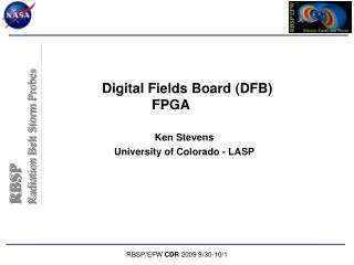
Polyimide Planarized DFB Laser Structure
top metal. top metal. p-InP. p-InP. n-InP substrate. n-InP substrate. polyimide layer. polyimide layer. Polyimide Planarized DFB Laser Structure. Farhan. Fabricated at the Semiconductor Laboratory at KTH in Stockholm. 1.7 m m. Harry. Finite Element Simulations. 5 0 -5
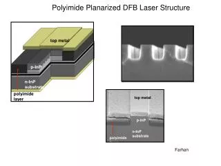

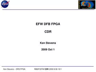
Polyimide Planarized DFB Laser Structure
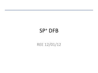
E N D
Presentation Transcript
top metal top metal p-InP p-InP n-InP substrate n-InP substrate polyimide layer polyimide layer Polyimide Planarized DFB Laser Structure Farhan
Fabricated at the Semiconductor Laboratory at KTH in Stockholm 1.7 mm Harry
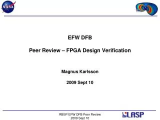
Finite Element Simulations 5 0 -5 -10 -150 -50 0 50 150 Kevin
2000 nm 200 nm Mathew
AFM and MFM Images Nanomagnetic Array AFM Height in nanometers MFM phase response in degrees Particles are single domain and the easy axis is to the sample plane. Mathew
Scanning Probe Microscope Mathew
Nanomagnetic Array Mathew
Current Imaging AFM MFM I I=50mA Lift height = 220nm Mathew
Dynamic Range of 850nm VCSEL 110 35 105 30 25 100 Bias (mA) Spur-Free Dynamic Range (dB-Hz2/3) 20 95 15 90 10 85 5 1 2 3 4 Frequency (GHz) Free space Harry