Download
1 / 15
160 likes | 346 Views
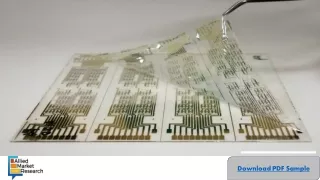
Solution processible Inorganic Nanocrystal based Thin-film Transistor. Hongki Kang. EE235 April 27 2009. Flexible Electronics. Polymer Vision: Readius. Printed Electronics. - Printable (=solution processible ) semiconductor material. Organic semiconductor

E N D
Solution processible Inorganic Nanocrystal based Thin-film Transistor Hongki Kang EE235 April 27 2009
Flexible Electronics Polymer Vision: Readius
- Printable (=solution processible) semiconductor material • Organic semiconductor • Unstable (H2O, O2 etc) • Low performance (≈ amorphous Si, mobility 1cm2/Vs) Flexible & Printed Electronics
Nano particle Sintering large surface-to-volume ratio
HgTe, HgSe • High mobility (µHgTe,p: 320cm2/Vs, µHgSe,n: 15,000cm2/Vs @300K) • Low melting point (Tm,HgTe: 670°C, Tm,HgSe: 799°C) • NC synthesis (diameter ~5nm) • -synthesized in an aqueous solution by a colloidal method • Solution A: Hg(ClO4)2 + 1-thioglycerol in DI water with NaOH in N2 • Gas B: H2Te gas (generated Al2Te3 + H2SO4 under N2) • Under stirring, Gas B was passed through Solution A • The precipitate containing thioglycerol-capped HgTe particles was separated by centrifugation. Process Flow (1)- Nanocrystal Synthesis
Process Flow (1) - Nanocrystal Synthesis - Single-crystalline - Transparent - sintering temperature ↑ => conductivity↑ optimized condition: @150 °C for 15 min
S G D HgSe Nanocrystals • Prohibiting the water vapor from penetrating the bare poly-ether-sulfone (PES) • Minimizing the damage of the PVP layers occurring during photo-resist development and lift-off processes • Cross-linked poly-4-vinylphenol (C-PVP) buffer layer on PES substrate (spin coating) • Gold gate electrode • (thermal evaporator) 65° • Al2O3 insulator • (atomic layer deposition) • Changing the layers into hydrophilic easily and rapidly • Patterning • (photolithography) • UV/ozone treatment (a) Before UV/ozone treatment (b) After UV/ozone treatment • HgTE/HgSenanocrystal channel layer • (spin coating) • A HgSe nanocrystal-based flexible TFT • Lift-off process • Sintering process • at 150 oC for 15 minutes • Source/drain electrodes • HgSenanocrystal-based • thin film transistor (TFT) Process Flow (2) - Device Fabrication
<HgTe> <HgSe> Device Characteristic
Mobility: better than organic semiconductor, a-Si • Thermal budget: compatible with plastic substrate • Stability: Air stable • ION/IOFFratio: low Result
Flexible & Printed Electronics • Optimization • Printability • More material research • Material Compatibility Conclusion
Thanks, Questions? Conclusion