Download
1 / 13
130 likes | 225 Views
Learn how to achieve good signal routing with equal lengths and uniform power bus routing for reliable circuit performance. Discover the importance of ionic cleanliness and managing organic acids in solder masks, such as acetate and formate, bromide, chloride, nitrate, ammonium, sulfate, sodium, potassium, calcium, and magnesium levels. Explore the significance of citrate in gold plating solutions and IPC-6012 standards for ionic cleanliness. Find insights into Low Signal, High Bias, and High Reliability Designs with specific Thru-Hole and Surface Mount Technology component packages like Axial Leaded, Radial Leaded, T0 Series, T0-92, T0-220, T0-3, DIP, SIP, SMT, SOT, QFP, PLCC, and BGA. Improve your PCB design practices with this comprehensive guide!

E N D
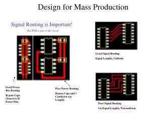
Signal Routing is Important! The PCB is part of the circuit Good Signal Routing Equal Lengths, Uniform Good Power Bus Routing Bypass Caps Closest to IC Power Pins Poor Power Routing Bypass Caps and 1 Conductor too Lengthy Poor Signal Routing Un-Equal Lengths, Non-uniform
PCB Ionic Cleanliness is Important • Acetate & Formate - These organic acids can be extracted from some solder masks. High levels can be indicative of an incompletely cured solder mask. Incomplete cure can allow exposure of the copper traces to the environment resulting in corrosion and board failure. • Bromide: Brominated compounds are added to laminates as a flame retardant. Some laminates are employing alternate, non-bromine, flame retardants. These are usually called specified as containing non-halogen flame retardants. The surface bromide concentration is a function of the laminate heat history. Bromide has also been identified as a component in some marking ink formulations and some solder masks. • Chloride - Chloride ions are the single most damaging material that can be on the board. High levels are usually due to insufficient washing prior to applying the solder mask. Chloride can also be transferred to the board by handling. • Nitrate and Ammonium - Both of these can be introduced in various plating processes. • Sulfate - Sulfate is rarely a problem. High levels are usually caused by poor housekeeping: dirty equipment, unpainted walls or unsealed floors. • Sodium & Potassium - Sodium can be induced by handling but is also a component of tap water and may be indicative of poor water treatment. In this case, chloride, calcium and magnesium should also be present. • Calcium and Magnesium - Calcium and magnesium come from rinse water and are indicative of poor water quality. • Citrate - Citrate salts and acids are components of some gold plating solutions. They also are in many environmentally friendly cleaners. IPC-6012 mandates the total ionic cleanliness prior to solder mask be <10ug/in2 in NaCl equivelants (IPC-TM-650) Most Low Signal Or High Bias, High Reliability Designs Require Much Lower Levels on Individual Ions
Thru-Hole Device Packages • Passives and Discretes • Axial Leaded (2 terminal, lying down) • Resistors, Capacitors, Inductors, Diodes • Radial Leaded (2 terminal, standing up) • Capacitors, Inductors, LEDs, MOVs, Power Resistors, … • T0 – Series (2-N terminals, Most Accommodate Std Heat Sink hardware) • T0-92 Small Signal Transistors, Regulators, References • T0-220 Moderate Power (~1W) Transistors, Regulators, Amplifiers • T0-3 Higher Power (~3W) Transistors, Regulators, Amplifiers
Thru-Hole Device Packages • Integrated Circuits, Resistors, Relays • DIP (Dual In-Line Package) • PDIP, CDIP • SIP (Single In-Line Package) • Rectangular
SMT – Surface Mount Technology Generations 20mm DIP Small Outline Package Shrink SO Package Thin Shrink SOP Depopulated, Very Thin, Quad Flat Pack, No Leads 3 mm