Physical Data in High-Tech Integration
350 likes | 378 Views
Explore the significance of physical data in top-level integration, SDF data, parasitic models accepted by PrimeTime, and more. Gain insights on timing convergence, back-annotation, and various RC network formats. Enhance your knowledge of net delays and interconnect issues. Dive into precise models like Lumped RC, Reduced RC, and Detailed RC for accurate parasitic back-annotation. Discover the impact of net topology modeling on circuit timing.

Physical Data in High-Tech Integration
E N D
Presentation Transcript
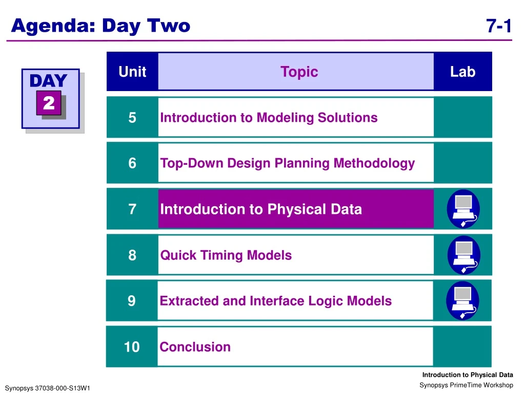
Agenda: Day Two Topic Unit Lab DAY 2 Introduction to Modeling Solutions 5 Top-Down Design Planning Methodology 6 Introduction to Physical Data 7 Quick Timing Models 8 Extracted and Interface Logic Models 9 Conclusion 10
Unit Objectives • State why physical data is useful during top-level integration • State what is SDF data • State the three parasitic models PrimeTime accepts • State the precedence of back-annotated data After completing this unit, you should be able to:
Why Use Physical Data? Why use physical data? Creating Quick Timing Mode and its Application Introduction to physical data Advantages of Timing Models Resolve some issues with back-annotation Advantages of Timing Models
Timing Convergence • The goal is to achieve timing convergence with the physical tools • Without timing convergence, there may be many iterations between the logical and physical tools before timing closure! • Execute top-level integration with available physical data • Prelayout, timing analysis performed based on wire load models • Postlayout, replace wire load models with actual net parasitic data
The Limitation of Wire Load Models Logical Design PrimeTime assumes the circuit looks like this: All nets (fanout = 1) except sel: length = 0.39 (from wire load model) sel: (fanout = 2) length = 0.86 (from wire load model) b n1 y sel a n2 Physical Design Even though, after layout, it may look like this: n1 b netlength a 0.41 b 0.41 sel 0.90 netlength n1 0.35 n2 0.97 y 0.38 y sel n2 a
0.5 1.0 The “Cost” of Estimating Net Delays • In large geometries, net delay was only a small portion of a path’s total delay • Estimating the timing of a “low impact” portion of the circuit is OK • In smaller geometries, delays due to net capacitance are a large portion of the path delay Unknown delay during compile Delay due to interconnect is up to 70% of the total delay Delay Interconnect delay Cell delay Technology 0.2 Device gate length
Introduction to Physical Data Why use physical data? Creating Quick Timing Mode and its Application Introduction to physical data Advantages of Timing Models Resolve some issues with back-annotation Advantages of Timing Models
0.02 0.03 0.02 0.02 0.02 0.08 Parasitic versus SDF • SDF back-annotation is used to describe net and cell delays • No cell or net delay calculation by PT - a “frozen” snapshot • Parasitic back-annotation is used to describe net resistance and capacitance (RC). RCs are used for • Performing design rule analysis (for example, max_capacitance) • Computation of cell and net delays if no SDF is annotated • Using SDF will be faster than delay calculation with parasitics • For multiple analyses on the same netlist, use PT to generate SDF for subsequent runs SDF Parasitics
Symbol Annotation H Hybrid annotation * SDF back annotation & RC network back annotation $ RC pi back annotation + Lumped RC <none> Wire load model or none report_timing with Physical Data report_timing now tags various symbols to indicate type of back-annotation information
Back-Annotation Command Summary • read_sdf • report_annotated_delay, report_annotated_check • remove_annotated_delay, remove_annotated_check • read_parasitics • report_annotated_parasitics • remove_annotated_parasitics
Third-Party Extraction Tools Parasitic Back-Annotation PrimeTime Timing Assertions PrimeTime Delay Calculator and Analysis Chip Architect, Arcadia Parasitic Back- Annotation RSPF/DSPF/SPEF Formats Timing Closure Tools
Different Parasitic Formats • set_load/set_resistance -- Lumped RC Model • SPEF -- Standard Parasitic Exchange Format (IEEE standard) • RSPF -- Reduced Standard Parasitic Format • DSPF -- Detailed Standard Parasitic Format
U2 U1 R = 0.12 NetA U3 C = 0.08 Lumped RC Data set_load 0.08 [get_net NetA] set_resistance 0.12 [get_net NetA]
More on Lumped RC • Lumped RC data is the simplest model which PT accepts for back-annotated parasitics • Entire net represented by a single capacitance and resistance • Limitations: • Does not model varying load placement • Does not model net topology • Can be pessimistic
+ + E1 E2 C4 C3 - - The Reduced RC Model read_parasitics myDes.rspf Elmore delay from U1 to U2 U2 R3 Driver U1 R1 Loads C2 (Cnear) C1 (Cfar) R4 U3 Elmore delay from U1 to U3
More on the Reduced RC Model • The reduced RC model is more accurate than the lumped RC model • Net RC represented by the Pi model • Cnear and Cfar model varying load placement. R provides resistance shielding • Limitations • Does not model net topology
R5 C3 C5 R3 C7 R1 R2 C2 C1 R4 R6 C4 C6 The Detailed RC Model read_parasitics myDes.dspf
More on the Detailed RC Model • The detailed RC data is the most accurate model PT accepts for back-annotated parasitics • Net RC represented by many Rs and Cs • Addresses net topology • Limitations: • Consumes most CPU time • Requires iterative calculations for each net • For more information read Delay Calculation with Detailed Parasitics, Appendix A in PrimeTime User Guide: Advanced Timing Analysis
Parasitic Trip-Point Parameters • PrimeTime environment variables have to be set to match the library characterization trip-points for SPEF/RSPF/DSPF • The default values for the variables are: rc_input_threshold_pct_fall = "50" rc_input_threshold_pct_rise = "50" rc_output_threshold_pct_fall = "50" rc_output_threshold_pct_rise = "50" rc_slew_lower_threshold_pct_fall = "20" rc_slew_lower_threshold_pct_rise = "20" rc_slew_upper_threshold_pct_fall = "80" rc_slew_upper_threshold_pct_rise = "80"
List of Precedence If SDF and parasitic data are both annotated, the order of precedence for timing analysis is as follows: • SDF • SPEF/DSPF/RSPF • Lumped RC • Wire Load Models
Resolve Some Back-Annotation Issues Why use physical data? Creating Quick Timing Mode and its Application Introduction to physical data Advantages of Timing Models Resolve some back-annotation issues Advantages of Timing Models
Missing Timing Arcs in SDF pt_shell> read_sdf AM2910.sdf Error: No net timing arc from pin 'U1/Z' to pin 'U2/A'.(PTE-014) Error: Cannot find pin ‘U10/CORE/Z’ in design AM2910 (DES-002) • Suggestions • Check for out-of-date SDF • Arcs in SDF must match arcs in library and design • Check SDF hierarchy separator is consistent with netlist • Some SDF writers won’t write delays below a threshold • PT will calculate delays. • Check path prefix is correct • read_sdf -path • read_sdf -strip_path
List Missing Timing Arcs in SDF report_annotated_delay -list_not_annotated **************************************** Report : annotated_delay -list_not_annotated Design : TOP **************************************** Non backannotated NETS from input ports: ---------------------------------------- 1. CARRY_IN -> U2/U73/B 2. CARRY_IN -> U2/U102/B 3. CLOCK -> U22/A | | | NOT | Delay type | Total | Annotated | Annotated | -----------------------------+-----------+-----------+-----------+ cell arcs | 1078 | 1065 | 13 | internal net arcs | 396 | 325 | 71 | net arcs from primary inputs | 44 | 0 | 44 | net arcs to primary outputs | 16 | 0 | 16 | -----------------------------+-----------+-----------+-----------+ | 1534 | 1390 | 144 | ...
Incomplete RC Network for DSPF How does PT handle incomplete DSPF back-annotated nets? PT discards the detailed RC network data and uses the wire load model pt_shell> report_annotated_parasitics -check Error: Driver pin 'U5/U200/Z' is not connected to RC network of net 'U5/n529’ RC network on that net is incomplete, so it is ignored. (DES-026) Error: Load pin 'U5/U200/A' is not connected to RC network of net 'INSTRUCTION[3]' RC network on that net is incomplete, so it is ignored. (DES-026)
Filling in Incomplete Net Parasitic Data • PT can fill incomplete parasitics with the following conditions • The segments that have physical data are from DSPF or SPEF • The complete missing segment is between two pins, hierarchical and leaf or hierarchical and hierarchical • Do not use to fix parasitic files with errors • Use only to fill the remaining, less significant segments of a net with zero or a wireload model read_parasitics spef_file.spef complete_net_parasitics [-complete_with zero|wlm] Missing Segments blockA blockB U2 U1 OUT IN
Unit Review • State why physical data is useful during top-level integration • State what is SDF data • State the three parasitic models PrimeTime accepts • State the precedence of back-annotated data
LAB Lab Overview and Review • Incorporate physical data into PT and perform STA • Explore the difference between parasitic data and SDF • Resolve one back-annotation issue 45 minutes Lab Review • Why is it important to understand and fix any missing physical data? • When using an SDF flow for timing analysis, what will PT use for design rule checks (for example, max_capacitance or max_transition)?
Plus! Additional Information... The information contained in the “PLUS!” section is intended to supplement the workshop material.
What Is PrimeTime-SI? • Extends PrimeTime’s ability to take into account the effects of crosstalk on timing • Crosstalk is a 1st order problem for 0.18micron and below! • Based on proven STA technology • Crosstalk analysis throughout the design process • Integration with implementation flow • Timing accurate • Low cost adoption • Multi-million gate capacity & performance + PrimeTime-SI Static Timing Analysis Static Crosstalk Analysis STA Technology with Crosstalk
What Is Crosstalk? • The electrical interaction that occurs between two or more nets • Causes: • Long parallel net • Coupling capacitance • High frequency switching Aggressor CS CW Victim Delay Variation Aggressor Noise/Glitch Victim
Volt Switching Threshold Time What Are Crosstalk Delay Effects? • Timing failures • Crosstalk affects interconnect delay of affected nets • Nets changing in the same direction: speed up • Nets changing in opposite directions: slow down • STA tools model cross-coupling capacitances as grounded capacitance only! Ideal waveform Speed-up Effect Slow-down Effect
Integrated Static Timing & Crosstalk Analysis State of the Solutions Static Crosstalk Analysis Traditional Bolt on Analysis Synthesis Physical Synthesis Physical Synthesis Place & Route Route Route Static Timing Analysis SPICE Simulation Crosstalk Analysis
Detailed Standard Parasitic Format (DSPF) *|DSPF 1.3 *|DESIGN "counter" *|DATE "Fri Jun 11 11:05:06 1999" *|VENDOR "Synopsys, Inc." *|PROGRAM "PrimeTime" *|VERSION "1999.10" *|DIVIDER / *|DELIMITER : *|BUSBIT "[]” .SUBCKT counter +A +B +C +QA *|GROUND_NET VSS * *|NET P 6.576586pF *|P (P I 0.000000pF) *|S (P:1 0.0 0.0) *|I (y:A y A I 1.000000pF 0 0) R0 P P:1 61.728001 R1 P:1 y:A 61.728001 C0 P VSS 1.858862pF C1 P:1 VSS 1.858862pF C2 y:A VSS 1.858862pF y P R0 R1 P:1 A C1 C0 C2
RSPF Example *|RSPF 1.3 *|DESIGN "counter" *|DATE "Fri Jun 11 11:07:35 1999" *|VENDOR "Synopsys, Inc." *|PROGRAM "PrimeTime" *|VERSION "1999.10" *|DIVIDER / *|DELIMITER : *|BUSBIT "[]" .SUBCKT counter +A +B +C +QA *|GROUND_NET VSS *|NET b 1.000000pF * *|DRIVER ffa:Q ffa Q *|S (b:1 0.0 0.0) R1 ffa:Q b:1 50.000000 C1 ffa:Q VSS 0.057990pF C2 b:1 VSS 0.102600pF *|LOAD QA:A QA A *|S (b:2 0.0 0.0) E1 b:2 VSS ffa:Q VSS 1 R1 b:2 QA:A 0.000000 C1 QA:A VSS 1pF Header info Port info Net name and Ctotal Driver, R1, C1, and C2 Load Voltage, R and C
Appendix: SDF & SPEF IEEE Format Specs • SPEF (Standard Parasitic Exchange Format) IEEE 1481-1998 http://www.eda.org/dpc/dpc-pandc/index.html • SDF (Standard Delay Format) http://www.eda.org/sdf • Cadence • DSPF (Detailed Standard Parasitic Format) • RSPF (Reduced Standard Parasitic Format)


