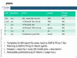
TLU plans
TLU plans. Motivation. Have a compact trigger logic unit in one board instead of tens of VME modules and lemo cables dangling around. Easy configuration of trigger logic remotely with added functionalities such as test readout elements (TimePix + DUT) without beam (ie auto trigger).

TLU plans
E N D
Presentation Transcript
TLU plans D. Esperante, Velo upgrade meeting
Motivation • Have a compact trigger logic unit in one board instead of tens of VME modules and lemo cables dangling around. • Easy configuration of trigger logic remotely with added functionalities such as test readout elements (TimePix + DUT) without beam (ie auto trigger). • Make the logic a bit generic such it can be attached to LHC like read-out systems. • Implement a TDC that provides timing information. D. Esperante, Velo upgrade meeting
General scheme (1) Control PC Readout PC Ethernet Control data GBE TLU data External input trigger signals from NIM logic Embedded system based on Altera Stratix II FPGA development board External veto signals Output trigger signals to telescope + DUT D. Esperante, Velo upgrade meeting
General scheme (2) Ethernet Control data via webservices GBE TDC data (tobedefined) DMA SRAM (TDC data) NIOS II processor External input trigger signals DMA SDRAM (control software) Veto/enable signals Coincidence signal sampling + TDC + trigger generator Output trigger signals D. Esperante, Velo upgrade meeting
Signaling example Spill Spill signal RO time Shutter signal Beetle trigger signal 40 MHz clock D. Esperante, Velo upgrade meeting
GPP: General Purpose Pulser Coincidences Synch trigger Enable signal Start dead-time Burst length Burst length Dead time Dead time Pulse output • General purpose pulser (GPP) • Programmable features: • Startup dead time. • Pulse length. • Inter-pulse dead-time. • Max pulse count. • Output delay in clock cycles. • With or without repetition. • Programmable multiplexor input to select several sources of enable/veto. • Programmable multiplexor input to select several sources of force cero output. • Force pull-down. D. Esperante, Velo upgrade meeting
GPP 2 • Using several GPPs with multiplexor at the enable/veto and “force-pull down” inputs we can implement the different output signals: • Spill signal: • Long burst length. • With repetition. • Timepix shutter signal: • Burst length modulated by external “force ‘0’ output”. • Dead time = timepix readout time. • Beetle trigger signal: • Burst length = ‘1’. • Dead time = ‘0’. • Max counter. • Veto/enable multiplexors: • The Spill signal enables the “Timepix shutter” and the “Beetle trigger” signals. • The “Beetle trigger” max counter forces the pull-down of the “Timepix shutter”. D. Esperante, Velo upgrade meeting
Internal scheme (1) Coincidence signal sampling + TDC + trigger generator CLK160 CLK80 CLK40 CLK40 TDC1 CLK20 EN Force pull-down CLK40 Max-cnt General purpose pulser (GPP) Coincidence RST CLK40 Shutter Signal detection and synchronization EN Force pull-down External veto/enable CLK40 General purpose pulser (GPP) Max-cnt Internal pulse generator RST 25ns trigger D. Esperante, Velo upgrade meeting
The TDC (‘s) • TDC • Features: • Implementation based on multiphase clock based on multiple of 40MHz (240 MHz). Resolution around 1ns. See “High-Precision TDC in an FPGA using 192-MHz Quadrature Clock”, Mark D. Fries, John J. Williams, Nuclear Science Symposium Conference Record, 2002 IEEE. 10/12/2002; 1:580- 584 vol.1. • 32-40 bits time counter. • Some extra bits with extra status info. To be defined. • The scheme also defines the signal synchronization circuitry. D. Esperante, Velo upgrade meeting
Time stamping of output signals • It may be helpful to record the time when a transition in any of the output signals ocurred. Two options: • A TDC per output signal. Too heavy. • Have a clock counter and use it as time stamp. Scatter-gather DMA TDC Time stamper CLK40 CLK40 Shutter Trigger D. Esperante, Velo upgrade meeting
Other technical issues • In this first design make something simple that works: • All clocks synchronous. • Will not use fancy improvements in the logic which would increase the data Tx rate. • Later improvements: • Think about an architecture that permits the TDC and the pulsers work in different clock domains so an external input clock could be used to generate the trigger signal while keeping the TDC untouched. • Zero-suppression… D. Esperante, Velo upgrade meeting
Other technical issues • NIM voltage levels compatibility: • Use LVPECL or build a small adapter board. • In the future, maybe we could build a plug-in board with the discriminators and coincidence units. • Output data format: • To be defined. • Software development needed: • Firmware for the embedded system. • TLU reader: the Rx software at the readout PC. • TLU controller: webservices based control (html page). D. Esperante, Velo upgrade meeting
Status • Embedded system with the NIOS II processor, SRAM, SDRAM, Ethernet link working. GBE not implemented yet. • Writing the VHDL for the pulser and performing the functional simulations. • Still quite a lot to do… • I’ll be away for some weeks… D. Esperante, Velo upgrade meeting