Download
1 / 26
260 likes | 390 Views
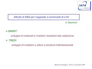
Attività di R&D per l’upgrade in luminosità di LHC. A. Macchiolo. SMART sviluppo di materiali e rivelatori resistenti alla radiazione TREDI sviluppo di rivelatori a silicio a struttura tridimensionale. Upgrade di luminosità di LHC- implicazioni per i tracciatori.

E N D
Attività di R&D per l’upgrade in luminosità di LHC A. Macchiolo • SMART sviluppo di materiali e rivelatori resistenti alla radiazione • TREDI sviluppo di rivelatori a silicio a struttura tridimensionale
Upgrade di luminosità di LHC- implicazioni per i tracciatori New layer inside the volume of the present pixel tracker Full Tracker Tracciatori a Super-LHC - L=1035 cm-2s-1 . • Layers interni r<20 cm: rivelatori a pixel su materiale rad-hard e/o nuove strutture (3D, epitassiale, diamante) • Layers intermedi : 20 < r < 60 cm micro-strip “corte” (2-3 cm) oppure macro-pixel su materiali più rad-hard (MCz) • Layers esterni: r> 60 cm micro-strip di lunghezza ~ 10 cm, tecnologia di LHC Anna Macchiolo Riunione Gruppo I, Firenze, 22 Gennaio 2007 Pixel Detector Inner Barrel (TIB) Endcap (TEC)
La Collaborazione SMART SMART: Structures and Materials for Advanced Radiation-hard Trackers Finananziata dal gruppo V INFN (2003-2006), lavora in sinergia con l’iniziativa RD50 del Cern Membri della collaborazione : 7 Istituti, 25 fisici Istituti fondatori: Bari, Firenze, Perugia, Pisa Istituti esterni: Padova, Trieste Istituzioni partner: IRST-ITC (Trento,Italy) Firenze: M. Bruzzi, D. Bassignana, E. Focardi, A. Macchiolo, D. Menichelli, C. Tosi Problematiche affrontate -Resistenza alla radiazione fino a fluenze di 1016 cm-2 Raggio < 20 cm il trapping è la maggiore limitazione, 20 cm< Raggio < 50 cm il problema principale è lo sviluppo della tensione di svuotamento con la fluenza Anna Macchiolo Riunione Gruppo I, Firenze, 22 Gennaio 2007
Materiali studiati in SMART • materiale MCz di tipo n e p: rappresenta una soluzione promettente per i layer intermedi: buona reperibilità e basso costo. -e’ disponibile da pochi anni con resistività abbastanza alte da permettere il suo uso in rivelatori per HEP. • il silicio MCz di tipo n ha una inversione di tipo del bulk assente o ritardata rispetto al Fz. • aumento più contenuto della tensione di svuotamento in funzione della fluenza e del tempo di annealing dopo irraggiamento con protoni • silicio epitassiale: - è una possibilità per i pixel dei layer più interni. • .Gli spessori epitassiali studiati variano da 25 a 150 mm, su un substrato di silicio Cz con bassissima resistività. • il minore segnale raccolto a causa del ridotto spessore è meno problematico ad altissime fluenze dove la raccolta di carica è comunque limitata a pochi decine di micron dal trapping. • migliore risposta ai neutroni di Fz e MCz
SMART: layout del wafer • Il layout del wafer è stato disegnato dalla Collaborazione SMART • Processato da ITC-IRST (Trento) • primi mini-sensori su silicio MCz di tipo p mai prodotti diodes MOS Micro-strip detectors Geometrie dei mini-sensori 100 mm pitch 50 mm pitch m (m m m -strip # pitch m) p+ width ( m) Metal width ( S1 50 15 23 S2 50 20 28 S3 50 25 33 S4 50 15 19 S5 50 15 27 S6 100 15 23 S7 100 25 33 RUN I p-on-n: 22 wafers Fz, MCz, Epi S8 100 35 43 S9 100 25 37 RUN II n-on-p: 24 wafers Fz, MCz S10 100 25 41 Passo / larghezza impianto p+ / larghezza metallizzazione sono variati intorno ai parametri scelti dai sensori di CMS: • Pitch/width=0.25 ottimizzazione della capacità inter-strip • Metal over-hang=11% dell’impianto p+ migliori performance riguardo al breakdown Anna Macchiolo Riunione Gruppo I, Firenze, 22 Gennaio 2007
Substrato di tipo p Rivelatori di tipo n-on-p (Fz o MCz) hanno migliori prestazioni per la raccolta di carica dopo l’irraggiamento be diminuisce annealing bh aumenta con l’annealing Vantaggi del substrato di tipo p (Fz o MCz): • velocità di drift me~3mh gli elettroni sono raccolti più velocemente e subiscono meno il trapping • non c’è inversione di tipo il campo elettrico rimane elevatp anche dopo le massime fluenze sul lato segmentato dei rivelatori Svantaggi: • Ancora non esiste una tecnica ottimale di isolamento delle striscie occore un tuning del p-spray e del p-stop per evitare bassi valori della tensione di breakdown prima e dopo l’irraggiamento • Il silicio MCz di tipo p presenta forti disomogeneità nella resistività di bulk a causa della formazione dei thermal donors durante il processo. Anna Macchiolo Riunione Gruppo I, Firenze, 22 Gennaio 2007
Secondo lay-out di SMART 4-inch process on p-type material • Small prototype of • CMS pixel • Atlas Pixel • (mask design by T. Rohe, PSI) IRST • “full size” detector: Mini-strip CMS/Atlas • Mini-strip : 80/100 micron pitch • 3 cm long • different implementations of the p-stop and p-spray techniques (p-stop width ranges from 5 to 25mm) Macro-pixel : 50 micron pitch • Commercial bump bonding and • connection routed as strip detectors (double metal technique) Anna Macchiolo Riunione Gruppo I, Firenze, 22 Gennaio 2007
Caratteristiche del layout: Pixels e Macro-pixels -Pixel CMS like on p-type bulk -Dimension as present CMS tracker devices(100 x 150mm2) -Standard (expensive) bump bonding -Single-side processing : n+ on p-type - Macro-pixel : 50 micron pitch 2 cm long - Commercial bump bonding and connection routed as strip detectors (Double metal technique) Anna Macchiolo Riunione Gruppo I, Firenze, 22 Gennaio 2007
Confronto di CCE su diversi materiali M. Bruzzi, 6th International "Hiroshima" STD06 Line to guide the eye for planar devices 160V [1] G. Casse et al. NIM A (2004) [2] M. Bruzzi et al. , this conference [3] G. Kramberger, RD50 Work. Prague 06 [4] W: Adams et al. NIM A (2006) [5] F. Moscatelli RD50 Work.CERN 2005 [6] C. Da Vià, this conference pixels strips Anna Macchiolo Riunione Gruppo I, Firenze, 22 Gennaio 2007
Rivelatori 3D Vantaggi Iniziativa “TREDI”, gruppo V INFN Sezioni INFN: Firenze, Trieste, gruppo collegato di Trento alla sezione di Padova Istituzioni collegate: ITC-IRST Gruppo di Firenze: M. Bruzzi, E. Focardi, A. Macchiolo, D. Menichelli, C. Tosi • la giunzione si sviluppa fra le colonne Tensioni di svuotamento limitate • Distanza di raccolta limitata ~ passo fra le colonne il trapping meno problematico e la raccolta di carica rapida • Lo spessore attivo rimane 300 mm alto segnale raccolto Svantaggi • Processo di fabbricazione con numerosi step alto costo rispetto ai dispositivi planari rivelatori a colonna rivelatori planari Anna Macchiolo Riunione Gruppo I, Firenze, 22 Gennaio 2007
particella ionizzante n+ electrodes n+ n+ p-type substrate Uniform p+ layer Single-Type-Column 3D detectors - Principio di funzionamento [C. Piemonte et al NIMA 541 (2205)] …passo intermedio sulla strada dei 3D standard:3D-STC gli elettroni sono raccolti velocemente grazie al campo trasversale le lacune driftano verso la zona centrale fra le colonne e diffondono verso il contatto p+ sul back • Il processo di fabbricazione è molto più semplice: • lo scavo delle colonne e il doping sono realizzati solo in uno step … … ma a causa del basso valore del campo elettrico nella regione centrale fra le colonne il meccanismo di raccolta di carica ha una coda temporale lenta Anna Macchiolo Riunione Gruppo I, Firenze, 22 Gennaio 2007
p-type columns Bulk contact 3-DDouble-SidedDouble-Type Columns lato giunzione identica a 3D-STC lato ohmico colonne senza read-out solo uno step di litografia necessario 50mm 300mm 50mm • 2 batches in fabbricazione : • configurazione p-on-n e n-on-p • lay-out con rivelatori a strip e a pixel Anna Macchiolo Riunione Gruppo I, Firenze, 22 Gennaio 2007
BACKUP Anna Macchiolo Riunione Gruppo I, Firenze, 22 Gennaio 2007
Oxygen concentration in FZ, CZ and EPI • Epitaxial silicon • Cz and DOFZ silicon EPIlayer • CZ: high Oi (oxygen) and O2i (oxygen dimer) concentration (homogeneous) • CZ: formation of Thermal Donors possible ! CZ substrate [G.Lindström et al.,10th European Symposium on Semiconductor Detectors, 12-16 June 2005] • EPI: Oi and O2i (?) diffusion from substrate into epi-layer during production • EPI: in-homogeneous oxygen distribution • DOFZ: inhomogeneous oxygen distribution • DOFZ: oxygen content increasing with time at high temperature SIMS profiling: [O](25µm) > [O](50µm)>[O](75µm) Anna Macchiolo Riunione Gruppo I, Firenze, 22 Gennaio 2007
In the MCz technique a magnetic field is applied : • Strongest field at crucible corner • flow suppressed by strong field => growth effectively from smaller, less unstable melt • better dopants and oxygen distribution with respect to Cz High resistivity MCz Wafer production 150 mm with reproducible resistivity vs. crystal length MCZ growth • high purity silica crucible • polysilicon grade comparable to high resistivity FZ [O] donor compensation Contamination from metal levels have been stable at or below detection limit of 109 at /cm2. O.Anttila, Okmetic Ltd., 6th RD50 - Helsinki, 2-4 June, 2005. http://rd50.web.cern.ch/rd50/6th-workshop/default.htm Anna Macchiolo Riunione Gruppo I, Firenze, 22 Gennaio 2007
Production Process Fz Samples MCz Samples • <100>ρ>500 W.cm thick=300mm • Standard: LTO, sintering @ 420C • no LTO (pass. layer), sint. @ 380C • no LTO, sintering @ 350C • no LTO, sintering @ 380C + TDK RUN I p-on-n 22 wafers Fz, MCz, Epi • <111>ρ>6KΩ*cm thick=300μm • Standard Process • sintering @ 380C • <100>ρ>1.8 KW*cm thick=300μm • No over-glass passivation • Low dose p-spray (3.0E12 cm-2) • High dose p-spray (5.0E12 cm-2) • <100>ρ>5KΩ*cm thick=200 mm • Low dose p-spray (3.0E12 cm-2) • High dose p-spray (5.0E12 cm-2) RUN II n-on-p 24 wafers Fz, MCz Anna Macchiolo Riunione Gruppo I, Firenze, 22 Gennaio 2007
Double junction model • E(x) highly non-uniform in heavily irradiated detectors due to the electrons and hole trapping by Deep Levels defects • close to the p+-contact the positive charge accumulated by deep donors will be higher than the negative charge accumulated by deep acceptors for the non-uniform distribution of free carriers. • The effect is the presence of two peaks in the electric field distribution. • SMART n-type MCZ samples • Double junction effect has been observed starting fromF=3×10¹⁴neq/cm2after irradiation with 24 GeV protons • At the fluence F=1.3×10¹⁵neq/cm2the dominant junction is still on the p+ side Technique: TCT set-up in St.Petersburg. A 830 mm laser induces a current pulse after illumination from the front side. The laser only travels a few microns in the silicon. The current pulse is created by the transport of electrons (holes are absorbed by the p+ implant). Electric field distribution extracted by means of a fit to the current pulse shape. M. Scaringella et al., NIM A (2006) p+ implantation n+
Charge collection After high radiation damage charge collection will be reduced by carrier trapping: be has beneficial annealing, conversely for bh • Drift velocity ( me~3mh ) electrons need smaller collection time • The drift of electrons will be completed sooner and consequently less charge will be trapped! • n+ readout better performing • n-in-p: - no type inversion, high electric field stays on structured side - collection of electrons G. Casse et al., NIMA535(2004) 362 • Miniature n-in-p microstrip detectors (280mm) • Detectors read-out with LHC speed (40MHz) chip (SCT128A) • Material: standardp-type and oxygenated (DOFZ) p-type • At the highest fluence Q~6500e at Vbias=900V Anna Macchiolo Riunione Gruppo I, Firenze, 22 Gennaio 2007
CCE on SMART p-type MCz Si diodes CCE Tested 700 600 500 400 SMG16 f=0.68E15 Depletion Voltage (V) SMG12 f=5.4E14 SMG10 f=4E14 SMG7 f=2.7E14 300 SMG5 f=2E14 SMG4 f=1.4E14 SMG26 f=1E14 200 300 SMG2 f=0.68E14 SMG1 f=0.4E14 100 0 0 50 100 150 200 250 300 Annealing time (min) non-irradiated at full depletion voltage 26MeV proton; 6.8x10¹⁴ 1MeV ncm-2; 750V; -30°C • Imax = 10A Vmax = 1000V • ENC 1500-2000e- • operation temperature down to - 30 °C • 90Sr source - analog DAQ with AC-coupled and shaping time of 2.4ms. % M.Bruzzi et al, 6th International "Hiroshima" STD06, Carmel Mission Inn, California September 11-15, 2006 Anna Macchiolo Riunione Gruppo I, Firenze, 22 Gennaio 2007
CCE on SMART n-type epi Si diodes Measurements after neutron irradiation: • Same CCE set-up as for the previous CCE measurements except for the shaping time reduced to 200ns. • After having normalized for the different thickness the collected signal before irradiation is the same for Fz and epitaxial material • about 6800 electrons collected in 150 mm thick epitaxial material after F=4×10¹⁵ neq/cm2 not-irradiated samples:epi and Fz 6800 electrons Anna Macchiolo Riunione Gruppo I, Firenze, 22 Gennaio 2007
Process Details of the new SMART production “New ” IRST Standard Process: • Aluminum sintering at 350 oC • low dose p-spray (3.0x1012 cm-2 ) • overglass passivation (SiO2 at T=300oC) • Silicon Nitride and poly-silicon deposition at ~ 700oC • Process Splittings: • 12 MCz p-type wafers:bulk resistivity >2KW.cm • 2 without nitride deposition (in coupling capacitors) • 2 without nitride and poly-silicon (bias resistors) deposition • 2 with standard process • 6 with Rapid Thermal Annealing before Aluminum sintering (try to annihilate Thermal Donors) • 7 p-type Fz : bulk resistivity 5-7 KW.cm • 4 standard wafers • 3 oxygenated wafers • 5 p-type epitaxial wafers:100 mm active thickness • epi layer resistivity ~300 W.cm Anna Macchiolo Riunione Gruppo I, Firenze, 22 Gennaio 2007
The Transient Current Technique Technique: TCT setup at IOFFE (St. Petersburg) TCT setup response 0.8 ns Temperature range 77 – 373K Laser wavelength 830um Laser induced current pulse shape: illumination from the front side. The laser only travels a few microns in the silicon. The current pulse is created by the transport of electrons (holes are absorbed by the p+ implant). Electric field distribution is extracted with a fit, taking into account the charge trapping • E(x) highly non-uniform in heavily irradiated detectors (electrons and hole trapping due to DLs): close to the p+-contact the positive charge accumulated by deep donors will be higher than the negative charge accumulated by deep acceptors. This is due to the non-uniform distribution of free carriers. The effectis the presence of two peaks in the electric field distribution. • Reverse current flow induces a relevant electric field Eb into the neutral base, that induces the drift of the collected charges through the base region. The response of the induced current pulse can be simulated as the result of the current drift through the entire thickness of the detector. Anna Macchiolo Riunione Gruppo I, Firenze, 22 Gennaio 2007
strip 1 strip 2 oxide n+ n+ e strip 1 strip 2 oxide oxide n+ n+ n+ n+ h VJBR no impact ionization model enabled VBR Impact ionization enabled p-spray breakdown • Three p-spray peak concentrations: • Np1=4e16cm-3 • Np2=8e16cm-3 • Np3=12e16cm-3 VJBR= potential difference between p-spray and strip which causes breakdown VBR= bias voltage for which we reach VJBR High Np => Low VJBR => Low VBR Transition voltage depends on the substrate concentration Slope depends on w/p Vbr increases for increasing Qox because VJBR increase Anna Macchiolo Riunione Gruppo I, Firenze, 22 Gennaio 2007
high-field regions S1 S2 S1 S2 S1 S2 p-stop Breakdown Similar approach to p-spray: 1. determine Vp-spray = f(VBIAS) 2. determine VJBR level increasing p-stop width VJBR VJBR • p-stop potential is higher • for wide implants • better narrow p-stop from the breakdown viewpoint Anna Macchiolo Riunione Gruppo I, Firenze, 22 Gennaio 2007
Combined p-spray p-stop p-spray: VBR - low before irradiation - improves for increasing QOX Cint - improves with irradiation BUT possible loss of isolation p-stop: VBR - high before irradiation - decreases for increasing QOX Cint - high and deteriorates for inc. QOX improves with QOX deteriorates with QOX • third solution is to combine the previous two using: • medium dose p-spray (to have sufficiently high initial VBR) • 20/30mm wide p-stop (to have low capacitance for high QOX) Anna Macchiolo Riunione Gruppo I, Firenze, 22 Gennaio 2007
high-field regions high-field regions high-field regions 3 5 4 1 2 S1 p-stop S2 S1 p-stop S2 S1 p-stop S2 Breakdown For increasing QOX: VBR first increases (typical of p-spray) than decreases (typical of p-stop) as QOX grows Anna Macchiolo Riunione Gruppo I, Firenze, 22 Gennaio 2007