Download
1 / 40
400 likes | 650 Views
Developments in electronics: CMOS scaling The quest for single electron sensitivity: avalanche gain vs electronic noise and detector capacitance A neglected technology: Interconnections Matching electronics and detector technology.

E N D
Developments in electronics: CMOS scaling The quest for single electron sensitivity: avalanche gain vs electronic noise and detector capacitance A neglected technology: Interconnections Matching electronics and detector technology Electronics for RICH DetectorsVeljko Radeka, BNLRICH 2004 Workshop
Acknowledgements: • Gianluigi De Geronimo • Paul O’Connor • Sergio Rescia • Pavel Rehak • Craig Woody • Bo Yu … my BNL colleagues.
Developments in electronics: CMOS scaling The quest for single electron sensitivity: avalanche gain vs electronic noise and detector capacitance A neglected technology: Interconnections Matching electronics and detector technology Electronics for RICH Detectors
CMOS Technology Roadmap • Driven by digital VLSI circuit needs • Goals: in each generation • 2X increase in density • 1.5X increase in speed
CMOS scaling: Oxide Thickness:
DVT Threshold mismatch due to discrete dopant distribution 3D p-MOSFET simulation with stochastically placed dopants D.J. Frank, IBM J. Res. Dev. 46, 235-244, Mar./May 2002
But: Gate tunneling current!!! • Gate current expected to increase 100 – 200 x per generation below 0.18 mm • Jox ~ 100 A/cm2 projected for Lmin = 0.1 mm generation with nitrided SiO2 • Considered tolerable for digital circuits (total gate area per chip ~ 0.1 cm2) • Typical CSA input FET would have IG ~ 1 - 10 µA; ENCp ~ 2000 - 7000 rms e- at 1 µsec • Good for radiation resistance – bad for ENC. SiO2 gate leakage current (Lo et al., Electron Dev. Letters 1997)
200x More Logic plus memory, µP, DSP, MGT 40x Faster 50x Lower Power per function x MHz 500x Lower Cost per function FPGAs - Thirteen Years of Progress P. Alfke
Higher Leakage Current… High Leakage current = static power consumption Was <100 microamps, now > 100 mA, even amps (!) Caused by: • Gate leakage due to 16 Å gate thickness • Sub-threshold leakage current incomplete turn-off because threshold does not scale Tyranny of numbers: 10 nA x 100 million transistors = 1 A evenly distributed, thus no reliability problem Sub-100 nm is not ideal for portable designs P. Alfke
VLSI ASIC Costs …. Mask set >$1M + design + verification + risk Source:IBM P. Alfke
Custom monolithics: technology access Multiproject foundry services • Combine designs from many institutions on one maskset • Arrange for regular runs with a variety of popular foundries • Design support • Models • Design rules • Process monitoring • Amortize cost of run over many users multiproject wafer
Front-End Electronics – Preamplifier Power • 32-channel ASIC - layout is pad-limited 3 x 3 mm² • power / channel 1mW (preamplifier < 200µW) • energy resolution < 250 rms electrons (600ns peaking time, 5pF)
Developments in electronics: CMOS scaling The quest for single electron sensitivity: avalanche gain vs electronic noise and detector capacitance A neglected technology: Interconnections Matching electronics and detector technology Electronics for RICH Detectors
Single Electron Detection and Timing vsAvalanche Gain Gav Detection (Yes/No): Gav ≥ ~ 10 ENC/qe “Common” Timing: Gav ≥ (ENC/qe) (tp/σt) ; tp = peaking time after shaping > signal current width Optimum timing: ---------------------------------------- 1. Coarse timing: ~ 1 – 2 ns , for tp = 20ns → Gav ≥ 10 ENC/qe = 100 ns → ≥ 50 ENC/qe 2. Precision timing: ~ 100 – 200 ps , for tp = 20 ns → Gav ≥ 100 ENC/qe ENC = ? (Note: Optimum filter for timing is different from opt. filter for charge measurement)
Optimum ENC vs Input Capacitance 10 fF 10 pF Power Pd is in input leg only. Add minimum 30µW for signal processing
Optimum ENC vs Input Capacitance 10 fF 10 pF Power Pd is in input leg only. Add minimum 30µW for signal processing
“Why is the detector capacitance so important in determining the noise performance?” for white series noise for 1/f series noise =transistor carrier transit time ≈ Cgs/gm; tm= integration time ; Kfis the 1/f noise constant [Joules]; kB= Boltzmann constant. It is illustrative to express the noise performance in terms of signal and noise “energy” on the detector capacitance. From matched filter theory and the well known relations for ENC: Numerical (dimensionless) constants aw ,a1/f ,contain capacitance matching constraints (Cd/Cgs ratio), weighting function shapeparameters, but are independent of the transistor width. Amplifier noise energy referred to the detector capacitance is independent of the detector capacitance. The signal energy is inversely proportional to the detector capacitance. (Cd here includes stray capacitances.) For a “gut feeling”: Charge at higher potential energy is easier to detect – 1 electron on 1 atofarad (quantum dot) is readily detectable – while not so at higher capacitances. VR 06/17/04
Pixel density – detector trends pixels/cm2 Doubling every 5 months Year
Power density • On-detector power density is limited by cooling capability. • Electronics for high-density detector must be extremely low power.
Silicon sensor (for EXAFS spectroscopy) • 384 pixels • 1 x 1 x 0.25 mm Si pad detector • rate > 10 MHz/cm2 • 8.2 mW/chan • FWHM < 300eV, noise < 28 e- • preamps + digital integrated on-chip G. De Geronimo et al., Proc. PIXEL2002 International Workshop, Carmel, CA, 2002
Shaping time: Note: Optimized noise vs. power (MOSFET optimized at each power level and shaping time) Cd = 1pF 0.25 µm CMOS G. DE Geronimo, P. O`Connor
Developments in electronics: CMOS scaling The quest for single electron sensitivity: avalanche gain vs electronic noise and detector capacitance A neglected technology: Interconnections Matching electronics and detector technology Electronics for RICH Detectors
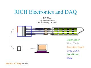
Detector – FE interconnect choices • board-to-backplane • easy to test, repair • large boards possible • connector pins are failure points • coarse pitch and high capacitance (> 1pF) • standard SMT package soldered to board (QFP or BGA) • easy to test, difficult to repair • capacitance down to 0.2 pF for small packages • board area limited by reflow oven capacity • wirebonded chip-on-board • difficult to test, assemble, and repair • board area limited by wirebonder • fragile • low capacitance (0.1 pF) • bump-bonded flip-chip • can match pixels with pitch from ~30 – 1000 mm • difficult to test, assemble, and repair • circuitry has to fit in same area as pixel • monolithic detector/electronics • interconnect is created as part of the detector fabrication process • ultra-low capacitance (few fF)
Interpolating Pad Readout for GEM (Gas Electron Multiplier) <100µm rms position resolution with 2mm pad pitch Window Upper GEM Lower GEM Anode Pad Plane
Time Projection Chamber (TPC) – (for Laser Electron Gamma Source) TPC Can double-GEM planes HV mesh plane and UV window for laser calibration anode pad plane electronics per pad ~ 8000 channels Spin ASYmmetry Array (SASY)
Board layout for a TPC – GEM anode plane. 32 channels per ASIC. ~ 8000 channels → ~ 10 watts on 35 cm dia plane
Board layout for a TPC – GEM anode plane. ASICS Blind vias GEM foils
ASIC Layout buffer channel • TSMC 0.25µm • 32 channels • 3.1 x 3.6 mm² (~0.35 mm2/channel) • 47k MOSFETs • 43mW • QFN package (56) bias logic
neighbors flag continuous reset threshold mux1 PD peak detector baseline stabilizer 2nd order shaper mux2 TD timing detector ramp • INPUT n-MOSFET • optimized for operating region • ENC<250 rms electrons • NIM A480, p.713 • CONTINUOUS RESET • feedback MOSFET • self adaptive • low noise • fully compensated • US patent 5,793,254 • NIM A421, p.322 • TNS 47, p.1458 • SHAPER • amplifier with passive feedback • dual stage multiple feedback • 2nd order, 600ns peaking time • adjustable channel gain (3-bit) • BASELINE STABILIZER (BLH) • band-gap referenced • low-frequency feedback • slew-rate limited follower • high dc stability < 1mV • low channel dispersion < 4mV • TNS 47, p.818 • PEAK DETECTOR • two-phase configuration • offset error cancellation • high absolute accuracy < 0.2% • US patent 6,512,399 • NIM A484, p.544 • TIMING DETECTOR • time-to-amplitude converter • internal or external ramp • two-phase configuration • timing resolution < 20ns rms 350 µW 900 µW ASIC Readout Channel - Block Diagram
Developments in electronics: CMOS scaling The quest for single electron sensitivity: avalanche gain vs electronic noise and detector capacitance A neglected technology: Interconnections Matching electronics and detector technology Electronics for RICH Detectors
GEM Readout of the HBD • Triple GEM • - can be made insensitive to charged • particles • - minimizes photon feedback and ion • backflow • Modest gain (~ 5 x 10³) • CsI photocathode deposited on top surface of uppermost GEM foil • CF4 used as working gas and Cherenkov • radiator - can achieve high gain and good • transmission down into deep VUV • ( large N0) Prototype HBD detector
~ ¾” honeycomb Readout Board and Preamps Preamp signals to shaper + ADC Hybrid Preamps with line drivers • Being developed by • BNL Instrumentation • Based on IO-535 • ± input signal • ± 2.5 V output wires Read pads ~ 3x3 cm2 GEMs • Need almost one full rack for the readout electronics
e+ e- q Pair Opening Angle The HBD Detector Electron pairs produce Cherenkov light, but hadrons with P < 4 GeV/c do not HBD Gas Volume: Filled with CF4 Radiator (nCF4=1.000620, LRADIATOR = 50 cm) Proximity focused Windowless Cherenkov Detector Radiator gas = Working Gas Cherenkov forms “blobs” on an image plane (Qmax = cos-1(1/n)~36 mradrBLOB~3.6cm) 55 cm 5 cm Coarse granularity readout (~ 2x2 cm2) Triple GEM detectors (8 panels per side) Space allocated for services Dilepton pair Beam Pipe
Low-Noise preamplifier – thick film ceramic hybrid • single channel • 29 components • 44 solder joints • 8 connections to PCB • 20 x 14 x 2.5 mm
N=1 N=9 N=25 N=49 Highly segmented detectors Benefits: • Position Resolution • pixel pitch ~ 1/N • Energy resolution (ENC) • CDET ~ 1/N • IDARK ~ 1/N • pulse shaping time ~ N • Rate capability • pileup ~ 1/N • “Small pixel” effect • improve energy resolution in semiconductor detectors with poor hole transport • Drawbacks: • Interconnect density~ N • → bump bonding; BGAs • Electronics channel count~ N • But these are not “old channels”! • Power/channel ~1/N • Noise is reduced more due to lower C, than increased due to lower power.
Concluding remarks: Microelectronics technology allows us to take advantage of fine electrode segmentation This leads to lower noise and lower avalanche gain Tough luck to very large electrode pads – not well matched to microelectronics Detector, detector electrodes, interconnections and the ASIC are all constituents of an interactive design. Scaling of digital electronics (powerful FPGAs) allows real time processing close to or on detector