Lecture 22
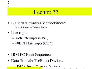
Lecture 22. IO & data transfer Methodolodies Polled, Interrupt Driven, DMA Interrupts AVR Interrupts (RISC) 68HC11 Interrupts (CISC) IBM PC Boot Sequence Data Transfer To/From Devices DMA (Direct Memory Access) Polled IO Interrupt Driven IO DMA, Polled, Interrupt Driven Summary

Lecture 22
E N D
Presentation Transcript
Lecture 22 • IO & data transfer Methodolodies • Polled, Interrupt Driven, DMA • Interrupts • AVR Interrupts (RISC) • 68HC11 Interrupts (CISC) • IBM PC Boot Sequence • Data Transfer To/From Devices • DMA (Direct Memory Access) • Polled IO • Interrupt Driven IO • DMA, Polled, Interrupt Driven Summary • Keyboard Input
Polled, Interrupt Driven, DMA • Polled IO: • A Device is polled thousands of times before data becomes available by the main program • Typically Wastes 99% or more CPU resource • Simple but inefficient • Sometimes needed for fast response and/or complex peripherals. For example a dedicated single-purpose controller. • Sometimes used when insufficient interrupts are available
Polled, Interrupt Driven, DMA • Interrupt Driven IO • Device interrupts normal program execution only when device needs CPU attention. • Interrupt Service Routine uses some CPU resource, with some overhead. • Useful for reasonably frequent events (hundreds to thousands of interrupt events per second). • An excessively high interrupt rate can slow down (or prevent) normal program execution (eg thousands of interrupts per second)
Polled, Interrupt Driven, DMA • DMA : Direct Memory Addressing • Hardware performs the data transfer • No CPU interaction requirement • Fastest data transfer rate. An order of magnitude faster than the fastest CPU instruction sequence • Does not always stop the CPU from executing its instructions - transparent DMA • CPU can optionally be interrupted upon DMA operation completion or not.
Interrupts The AVR is a Reduced Instruction Set Computer. The 68HC11 - Complex Instruction Set Computer - it performs many tasks before entering an interrupt - making it simpler & easier for programmers to code interrupt service routines. The programmer need not specifically save any registers as that is performed by the CPU. To limit the time required to service an interrupt, an AVR only performs the minimal functions necessary to enter the Interrupt Service Routine. Tradeoff - The programmer must be careful not to upset the main line code execution.
AVR Stack • The Stack Pointer – SP – is read/write accessible in the I/O space. (SPH / SPL) • The data SRAM can easily be accessed through the five different addressing modes supported in the AVR architecture.
AVR Stack • During interrupts and subroutine calls, the return address Program Counter (PC) is stored on the Stack. • The Stack is effectively allocated in the general data SRAM, and consequently the stack size is only limited by the total SRAM size and the usage of the SRAM. • All user programs must initialise the SP in the reset routine (before subroutines or interrupts are executed).
AVR Interrupts • During interrupts and subroutine calls, the return address Program Counter (PC) is stored on the Stack. • The CPU clears the I flag - preventing furthur interrupts - until the current one is serviced. • The status register - SREG - is not automatically stored when entering an interrupt routine and restored when returning from an interrupt. • This must be handled by Interrupt Service Routine software.
AVR Status Register • The AVR status Register – SREG – is defined as: • 7 6 5 4 3 2 1 0 Bit # • I T H S V N Z C SREG • 0 0 0 0 0 0 0 0 Initial Value
AVR Interrupt Vectors The most typical and general program setup for the Reset and Interrupt Vector Addresses in ATmega128 is: Address Labels Code Comments $0000 jmp RESET ; Reset Handler $0002 jmp EXT_INT0 ; IRQ0 Handler $0004 jmp EXT_INT1 ; IRQ1 Handler $0006 jmp EXT_INT2 ; IRQ2 Handler $0008 jmp EXT_INT3 ; IRQ3 Handler $000A jmp EXT_INT4 ; IRQ4 Handler $000C jmp EXT_INT5 ; IRQ5 Handler $000E jmp EXT_INT6 ; IRQ6 Handler $0010 jmp EXT_INT7 ; IRQ7 Handler $0012 jmp TIM2_COMP ; Timer2 Compare Handler $0014 jmp TIM2_OVF ; Timer2 Overflow Handler $0016 jmp TIM1_CAPT ; Timer1 Capture Handler $0018 jmp TIM1_COMPA ; Timer1 CompareA Handler
AVR Interrupt Vectors continued $001A jmp TIM1_COMPB ; Timer1 CompareB Handler $001C jmp TIM1_OVF ; Timer1 Overflow Handler $001E jmp TIM0_COMP ; Timer0 Compare Handler $0020 jmp TIM0_OVF ; Timer0 Overflow Handler $0022 jmp SPI_STC ; SPI Transfer Complete Handler $0024 jmp USART0_RXC ; USART0 RX Complete Handler $0026 jmp USART0_DRE ; USART0,UDR Empty Handler $0028 jmp USART0_TXC ; USART0 TX Complete Handler $002A jmp ADC ; ADC Conversion Complete Handler $002C jmp EE_RDY ; EEPROM Ready Handler $002E jmp ANA_COMP ; Analog Comparator Handler $0030 jmp TIM1_COMPC ; Timer1 CompareC Handler $0032 jmp TIM3_CAPT ; Timer3 Capture Handler $0034 jmp TIM3_COMPA ; Timer3 CompareA Handler $0036 jmp TIM3_COMPB ; Timer3 CompareB Handler $0038 jmp TIM3_COMPC ; Timer3 CompareC Handler $003A jmp TIM3_OVF ; Timer3 Overflow Handler $003C jmp USART1_RXC ; USART1 RX Complete Handler
AVR Interrupt Vectors continued $003E jmp USART1_DRE ; USART1,UDR Empty Handler $0040 jmp USART1_TXC ; USART1 TX Complete Handler $0042 jmp TWI ; Two-wire Serial Interface $0044 jmp SPM_RDY ; SPM Ready Handler ; ; RESET HANDLER: RESET:ldir16, high(RAMEND); Main program start out SPH,r16 ; Set stack pointer to top of RAM ldi r16, low(RAMEND) out SPL,r16 sei ; Enable interrupts <instr> xxx ; other instructions...
AVR ADC Interrupt The Analog to Digital Converter can be configured to interrupt the CPU upon completing a conversion. By setting the interrupt enable bit, ADIE, this will allow CPU interruption when the ADIF flag is set. Upon ADC conversion completion the interrupt flag, ADIF, will be set. Providing interrupts are enabled - the “I” bit is set in SREGS, the AVR CPU will complete execution of the current instruction, then mask interrupts (clear the I bit) and jump to the ADC Conversion Complete interrupt Vector.
Polled ADC Access // Read the AD conversion result unsigned int read_adc(unsigned char adc_input) { ADMUX=adc_input|ADC_VREF_TYPE; // Start the AD conversion ADCSRA|=0x40; // Wait for the AD conversion to complete while ((ADCSRA & 0x10)==0); ADCSRA|=0x10; return ADCW; }
ADC Interrupt Service Routine // Code Vision ADC interrupt service routine - ISR interrupt [ADC_INT] void adc_isr(void) { register static unsigned char input_index=0; // Read the AD conversion result adc_data[input_index]=ADCW; // Select next ADC input if (++input_index > (LAST_ADC_INPUT- FIRST_ADC_INPUT)) input_index=0; ADMUX=(FIRST_ADC_INPUT | (ADC_VREF_TYPE & 0xff))+input_index; // Delay needed for the stabilization of the ADC input voltage delay_us(10); // Start the AD conversion ADCSRA|=0x40; }
USART0 TX ISR #define TX_BUFFER_SIZE0 80 // USART0 Transmitter buffer char tx_buffer0[TX_BUFFER_SIZE0]; // USART0 Transmitter interrupt service routine unsigned char tx_wr_index0, tx_rd_index0, tx_counter0; interrupt [USART0_TXC] void usart0_tx_isr(void) { if (tx_counter0) { --tx_counter0; UDR0=tx_buffer0[tx_rd_index0]; if (++tx_rd_index0 == TX_BUFFER_SIZE0) tx_rd_index0=0; }; }
Memory Interfacing • We want U16, our 128KB ROM, to be enabled from E0000..FFFFF, (1110 0000 0000 0000 0000B .. 1111 1111 1111 1111 1111B). So we need to decode the top three bits A19..A17, and when A19..A17 = 111 the chip select must be active. GCS1# = NOT (A19 & A18 & A17) • As chip Select is active low, so we can simply use a 3 input NAND gate as shown:
DRIVERS • A hardware driver normally consists of 2 or 3 parts: • 1. An Application Program Interface • A set of system calls to access the peripheral. • For example to read data from the UART memory buffer. • 2. An interrupt Service Routine (ISR) • Manipulates the device to support the peripheral • For example reading data from a UART into a memory buffer.
DRIVERS • Sometimes an interrupt service routine may need to perform a long task in the handler. • In this situation the ISR could be split into two. The time critical part (Top Half) is executed immediately, and the less time critical part (Bottom Half) is scheduled to occur at a more appropriate time. • Example: When a network card receives data, it is moved into a buffer by the “Top Half”. Then the Bottom Half scheduled. When the Bottom Half executes it interprets the packet and sends the data to the appropriate socket, interface & task.
DMA refresh of DRAM • As previously mentioned the DMA controller is used to refresh Dynamic RAM. • Remember Dynamic RAM is constructed using Capacitive storage elements. The presence or absence of charge on the capacitor indicates a stored 1 or 0. Due to internal resistance, the charge leaks away. In order to avoid memory loss, the data is read & re-written many times per second. (Typically every few ms)
DMA refresh of DRAM • Remember Dynamic RAM also is addressed using Rows and Columns. • In the event that one byte from one column is read, the whole row is read and refreshed. • So to refresh all 256 rows x 256 columns (64KB) only takes requires 256 sequential address reads.
DMA refresh of DRAM • On an IBM PC the DMA controller has an Auto-Initialise Block transfer mode. The Current Address and Current Word Count register are automatically loaded from previously saved Base Word count and Base Address registers. • The (8253) timer 1 output is latched onto the DMA controller’s DMA REQuest line (DREQ0) (74LS74). (Reset by DMACK0)
DMA refresh of DRAM • As soon as the DMA controller receives the DMA REQuest signal (DREQ), the DMA controller requests control of the system BUS using the 80x86 HOLD line. • Upon HoLD Acknowledgment (HLDA line) from the CPU, the DMA controller performs sequential reads from memory. • This has the effect of refreshing all Dynamic RAM memory.
8237 DMA • The DMA controller may be configured to transfer data: • From Memory to Memory • From Memory to IO (MEMR# & IOW#) • From IO to Memory (IOR# & MEMW#) • When the DMA controller is used to transfer from Memory <-> IO device the transfer occurs directly without using any intervening storage.
8237 DMA • When the DMA controller is used to transfer from Memory <-> IO device. The device can perform a transfer every 2 cpu clock cycles • The REP MOVSB command can transfer a byte in a block in 17 clock cycles. • So the DMA controller’s data transfer rate is over 8.5 times faster than an 8088 can be.
DMA vs Interrupt-Driven I/O • Also, an interrupt service routine would require at least: (INT) 52 + (IRET) 32 + 3*PUSH (30) + 3*POP (24) = minimum overhead of 138 cycles = 28us. • The DMA controller has minimum latency as it will gain control as soon as the CPU asserts HLDA (300ns-1.6us).
DMA vs Interrupt-Driven I/O • During CPU HOLD, the CPU’s Execution Unit (EU) will continue executing instructions from its pipeline, until it requires access to the Memory or IO busses. So it is possible that the DMA cycles do not interfere with CPU execution at all.
80186EC DRAM Refresh • In the 80186/8EC there is a special purpose Refresh Control Unit for DRAM memory refreshing. • This device refreshes all rows by cycling through all DRAM rows in “dummy read” cycles. • In this CPU refresh activity has higher priority than: DMA, Most CPU cycles & HOLD/HLDA bus protocol.
80186EC DMA • In the 80186/8EC there is an enhanced DMA controller (20 bit counters) • It allows data transfer between memory & peripherals without CPU intervention • The DMA controller can access the entire memory in either byte or word increments.
80186EC DMA • The four DMA Channels can each accept requests from: • An external pin • The Serial Communications Unit • The Timer/Counter Unit • The CPU by direct programming • CPU can continue execution of instructions until the pre-fetch queue is empty or an external Memory/IO access is required.
Polled IO • Polled I/O is the repeated reading of external control units waiting for data to become available. • When data becomes available, it is transferred under program control. • Polled IO may be implemented simply • It is normal to poll the device thousands of times before data becomes available.
Keyboard Input • The IBM PC Keyboard includes an Intel 8048 micro-controller. • The keyboard is arranged as a capacitive matrix in columns & rows. • When a key is pressed its capacitance increases. • The 8048 as sequences through rows of keys and any capacitance change is sensed on the columns.
Keyboard Input • When a key press is sensed the Key pressed scan code is sent to the CPU. • When a key is released the Key Released scan code is sent to the CPU. • If a key is held pressed, a key pressed scan code is repeated. • The CPU is interrupted (IRQ1) upon each keypress/release
Keyboard Input • The Keyboard ISR is invoked directly by the PIC IRQ 1 which provides an interrupt Type Vector = 9. So INT 9 is executed. The Keyboard ISR saves characters into a 16 byte buffer. • To read the buffered keyboard characters we use INT 16H - BIOS Keyboard IO.
Polled Keyboard Input poll_ready: ;wait until key press/release IN al, 64h ; read status TEST al, l ; New ScanCode ready? JZ poll_ready ; no - poll again IN al, 60h ; get the key code MOV bl, al ; free al for in/out IN al, 61h ; send ACK OR al, 10000000B ; set MSB OUT 61h, al ; write back to port AND al, 01111111B ; clear MSB OUT 61h, al ; write back to port
Interrupt Driven IO • Interrupt Driven I/O is where an interrupt input is connected to a device output that signals when data is received. • For example a serial communications port interrupts on arrival of one or more characters • Upon interrupt, the current task is interrupted, and data is then transferred under program control by an Interrupt Service Routine (ISR).
8086 Interrupts • Different types of Interrupts • Hardware Interrupts - the 8259 PIC presents the one-byte interrupt number on the local bus • Software Interrupts • eg BIOS & DOS interface. • Predefined interrupts - Interrupt numbers are assigned and use automatic vectoring logic. • Eg INT 0 = DIVision by 0, INT 1 = Single step, INT 2 = NMI, INT 3 - One Byte, INT4 - Overflow
8086 Interrupts Hardware Interrupt Acknowledge Sequence (min mode).
DMA, Polled, Interrupt Driven Summary • Polled IO: • A Device is polled thousands of times before data becomes available by the main program • Typically Wastes 99% or more CPU resource • Simple but inefficient • Sometimes needed for fast response and/or complex peripherals. For example a dedicated single-purpose controller. • Sometimes used when insufficient interrupts are available
DMA, Polled, Interrupt Driven Summary • Interrupt Driven IO • Device interrupts normal program execution only when device needs CPU attention. • Interrupt Service Routine uses some CPU resource, with some overhead. • Useful for reasonably frequent events (say hundreds of interrupt events per second). • An excessively high interrupt rate can slow down (or prevent) normal program execution (eg thousands of interrupts per second)
DMA, Polled, Interrupt Driven Summary • DMA summary: • No CPU interaction requirement • Fastest data transfer rate. An order of magnitude faster than the fastest CPU instruction sequence • Does not always stop the CPU from executing its instructions • CPU can optionally be interrupted upon DMA operation completion or not.

