Download
1 / 45
460 likes | 685 Views
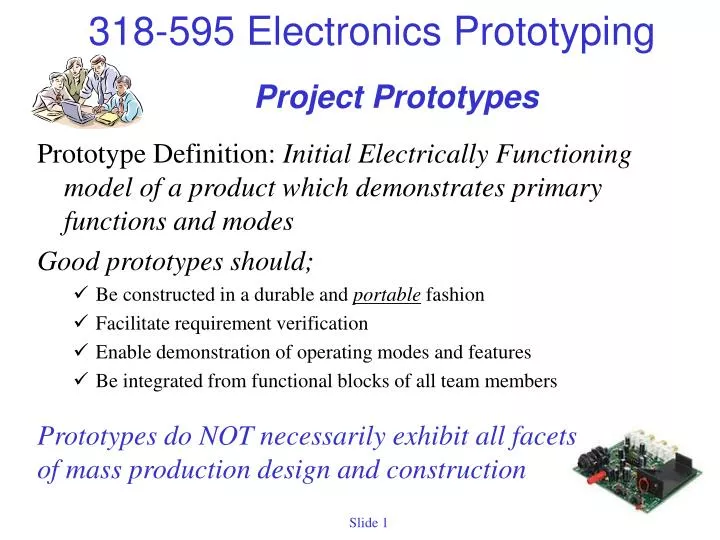
Project Prototypes. Prototype Definition: Initial Electrically Functioning model of a product which demonstrates primary functions and modes Good prototypes should; Be constructed in a durable and portable fashion Facilitate requirement verification

E N D
Project Prototypes Prototype Definition: Initial Electrically Functioning model of a product which demonstrates primary functions and modes Good prototypes should; • Be constructed in a durable and portable fashion • Facilitate requirement verification • Enable demonstration of operating modes and features • Be integrated from functional blocks of all team members Prototypes do NOT necessarily exhibit all facets of mass production design and construction
Prototype Production Design • One of a kind or few of a kind • Represents abstract of production design • Typically Thru Hole Components • Cost is not part of requirements allocation • Assembly process is not of interest • Assembly levels, PCBs do NOT match PD • Used for verification of requirements • Major Deliverables: Model • Working Demonstration Model • Demonstrate Major Functions • Minimal Documentation • Plan, Parts List, PCB Layouts • Demonstration Photos/Videos • Mass Production Quantities • Typically Use Surface Mount Technology • Mat & Asm Cost is an allocated requirement • Mat Cost use est annual production volumes • Define Assembly process flow diagram(s) • Define Assembly levels • Mfg test process part of Asm costs • Major Deliverables: Paper Exercise • Costed Bill of Materials incl package info • PCB Asm-Test Process Flow Diagrams • Assembly Level Diagram • PCB Layouts (optional) Both are Required
Basic Prototype Methods Breadboard or Plugboard Advantages • Solderless, Easy Mods • Very Rapid Prototyping • Well suited to TH 0.3” and 0.6” DIP IC’s & Low Power Discretes • Used in previous Labs Disadvantages • Holes limited to #18-22 AWG “solid” leads/wires on 0.1” centers • Circuit must be transported with extreme care • Boards are subject to wearout, wire breakages, warping, etc • Expensive, cumbersome for larger circuits • Not suited to SMT, connectors, displays, power devices, switches, etc • >10pF row-row capacitance
Basic Prototype Methods Wirewrap or Termipoint Advantages • Can be solderless or used in with solder • Relatively Rapid Prototyping • Well suited to DIP and SMT Conversions • Easy Mods but Very Reliable Disadvantages • All parts must fit into WW sockets/headers on 0.1” centers • WW Wire is small, #30 AWG, <100mA, 250nH/ft • WW Tool and special solid WW Wire required • Best Results with Pre-stripped Wire • Requires special WW sockets, bottom ID’s and perf board
Basic Prototype Methods Perfboard without Pads Advantages • Used with top or bottom side solder wire-wire connections • Can be used with DIP and SMT Conversion Sockets • Mods possible but require unsoldering • Reliable if used with hold down adhesives Disadvantages • All parts must fit into sockets/headers on 0.1” center hole pattern • Solder connections made with wire-wire or wire-pin • Insulation on wire connections can be compromised with heat • Slower than Wirewrap or solderless breadboard • Requires higher degree of soldering skills
Basic Prototype Methods Perfboard with Pads Advantages • Used with top or bottom side solder wire-wire connections • Can be used with DIP and SMT Conversion Sockets • Mods possible but require unsoldering pads (vacuum required) • Available with Gnd Planes, Power Traces/Busses • Better solder connections than w/o pads, More Reliable Disadvantages • All parts must fit into mountings on the hole pattern • More expensive than std perfboard • Slower than Wirewrap or solderless breadboard • Requires moderate degree of soldering skills
Basic Prototype Methods Deadbug Board Advantages • Access to connection side of all parts • Allows an excellent ground plane(s), Great for HF, VHF, UHF, RF • Copper board can be scraped to provide power traces as well • Inexpensive, Reliable if used with hold down adhesives Disadvantages • Part markings are upside-down • Not suited to digital or nodal intensive circuits • Requires adhesive to “deadbug” parts • Slow Method, Can be very delicate when part legs extend vertically • Requires very high degree of soldering skills
Basic Prototype Methods Printed Circuit Board – PCB Handmade – Transfer Artwork Process • Designer must utilize ruboff transfers, tape or pen hand lithography • Once design is transferred to Cu laminate, board is etched, then drilled Advantages • Mostly repeatable performance for RLC board effects • Can be used with or without component sockets, SMT or Thru Hole Parts • Relatively Fast Creation of Simple PCBs, less than 15 parts • High current capability for any conductor if properly designed • Good for power circuits, large copper area intensive circuits Disadvantages • For single or double sided boards only, No True Vias • Features less than 100mil spacing, 0805 discrete, 10mil trace very difficult • Use of etchants NH4Cl (Ammonium Chloride) or FeCl3 (Ferric Chloride)
Etching of Printed Circuits 1.5 Molar FeCl3 or NH4Cl CAUTION !! Developing and etching PCBs is a process that involves chemicals that dissolve metal (etching process). These chemicals can also burn your skin, have hazardous or toxic fumes, and can be absorbed under prolonged contact. In most cased these chemicals CANNOT and SHOULD NOT be disposed of by dumping into ordinary sanitary drains. PC etching should NEVER be done without adequate ventilation or in an area accessible by children, pets or other unsuspecting persons. Also these materials may stain or discolor flooring, furniture, and clothing. Follow ALL safety cautions mentioned on any etching materials purchased.
Basic Prototype Methods Printed Circuit Board – PCB Handmade – Photolithography Process • Designer must create photo lithograph “mask” of Cu circuit using eCAD • Positive or Negative Photo Sensitive Resist Cu laminate is then exposed (printed) to lithograph design, etched and drilled Advantages • Repeatable performance for RLC board effects • Can be used with or without component sockets, SMT or Thru Hole Parts • Fast assembly once PCB is created, drilled • High current capability for any conductor if properly designed • Good for Single and Double Sided boards Disadvantages • For single or double sided boards only, No Plated Holes or Vias • Use of etchants NH4Cl (Ammonium Chloride) or FeCl3 (Ferric Chloride)
Basic Prototype Methods Printed Circuit Board – PCB Outsourced Advantages • Professional, repeatable performance for RLC, mass producable • Can be used with or without component sockets, SMT or Thru Hole Parts • Fast assembly once PCB is procured • High current capability for any conductor • By far the most reliable prototype method • Circuit can be matched by computer to intended schematic Disadvantages • Procurement Time of PCB Fab takes ~1-2 weeks, (quick turn is an option) • Changes or mistake fixing can require “unsoldering” skills/tools • Extra Design Task of Creating Board Layout File/Artwork
10 Guidelines • Make good power supply and ground connections • A 30 AWG#, daisy-chained wire-wrap connection from chip to chip is very inadequate. For similar reasons to the decoupling, you must make low impedance power supply and ground returns. • For single and double sided boards use 20mil or larger (wider) traces. • For multilayer boards use separate planes for power(s) and ground(s) when possible • Check ALL wire & trace gauges for proper current capacity. • Decouple ALL IC power inputs • This includes analog, digital and data conversion IC’s • Employ a 0.1 uf ceramic capacitor from each supply to ground as close to the IC as possible. Switching internal to the IC can cause momentary voltage drops due to package and line length inductances. A local capacitor helps counteract this effect by providing local energy. • Include separate bypass capacitors for both the positive and negative supplies • Each circuit board should have additional “bulk” capacitors such as solid tantalum depending on local current draw
10 Guidelines • Keep digital and analog circuitry physically separated if possible • Digital switching, especially at microprocessor bus or video card speeds, can inject switching noise and other unwanted effects into analog circuitry. • When possible use separate analog and digital power and ground return runs, planes and/or wiring back to a central point as close to the DC power source as possible. This will keep the digital noise out of the analog circuitry. • Assume you may need to make changes! • Choose a suitable prototyping method that allow for changes, leave yourself enough space on your boards • Account for ALL your pins! • Terminate all unused inputs in some fashion which allows them to be utilized if needed without substantial rework. For example, spare op-amps can be terminated by creating unity gain followers and grounding the input. • Do NOT leave unused input floating unless the device is specifically designed for this condition.
10 Guidelines • Make sure your parts are available before locking in your design • Construct in circuit blocks • Construct and test functional blocks verifying performance as you go. Do NOT assemble more than a few blocks at a time before verifying functionality. The more circuits that are assembled and integrated, the harder it is to debug. • Whenever powering up circuitry the first time, ALWAYS check the DC supply current as the circuit powers up with your hand on the ON/OFF switch. If there is a wiring or connection mistake, many times it shows up as an over current scenario. Be ready to turn off the supply in the event of an overcurrent. • Cleanliness of circuits is essential for low signal analog performance • Don't use silicon sealant to tie down high-impedance or low current analog circuits! It may leave ionic laiden residue that can leak small currents which may be detrimental to circuit performance. • Use IC sockets on prototypes along with Thru-Hole technology if possible. • The “product” design can be very different in its packaging technology. Do NOT assume you need to use the same IC packages in your prototype. • Treat the PCB and other interconnect systems as part of the circuit design. • All PCB’s, wiring, breadboards, etc have resistance, capacitance and inductance
Soldering • Common Eutectic Solder types: • Solid Core: Mixture of ~63%Sn, ~37%Pb (183oC melting pt) • Acid Core (Not for electronics) • Flux Core (Rosin paste) • Solder Iron Types: • Pencil (AC powered) w/o temp control (15-30 Watts) • Pencil (AC powered) with temp control (variac) • Gun (AC powered) with temp control (used for larger applications) • LP pencil or gun (Butane or LP powered) • Soldering Tips are usually detachable/replaceable, must be kept clean by using a wiping system (damp sponge or rag). When fully powered, many soldering devices will ignite paper, wood and other combustables …… caution • Soldering should be done on a non-combustable surface • The iron is used to heat the metal parts that are to be joined by surface contact. • The tip of the iron should be solder “wetted” in order to transfer heat to the parts more efficiently with the surface contact. • The wire solder is then touched to the side opposite to the heat application. If of sufficient temperature, the solder will melt and “flow” toward the heat source. • All metal surfaces to be joined need to be clean. If coated with any corrosion or oils, the process will not work or be prone to early failures Note: Some Solders Contain Lead Always Wash Hands After Contacting! Solder Pump Removal Tool
Best Practice Steps to SolderingFacilities and Equipment • ESD and heat protective lab bench top • Heated Soldering tool (25W min iron) with small tip for electronic work • Adequate ventilation • Safety glasses and other protective clothing/equipment • Small gauge #18AWG or smaller Sn63Pb37 rosin core solder wire • De-soldering tool (wire braid or suction tool)
Best Practice Steps to SolderingTechnique and Process • Make certain contact surfaces of components are clean and free from dirt, oils or oxides • The component contact surfaces need to be thermally connected. Clamp if necessary. • Allow the soldering tool to heat to proper temp (Sn63Pb37 solder melts at 183oC) but the soldering tool tip should be at least 350oC (Pb free solders usually higher by ~40oC) • "Tin" the iron tip with a small amount of solder. Critical when using a new tip or iron. • Clean the tip of the hot soldering iron on a damp sponge or cotton rag • Melt a small amount of solder on the tool tip again. • Heat the contact surface by touching the melted solder coated tool tip to the surfaces for one to two seconds (longer contact may risk damage to parts) • Immediately melt additional solder wire by touching the solder wire to the OPPOSITE side of the contact surfaces. Add only enough solder to form an adequate joint. • Remove both iron and solder wire and return the iron safely to its stand. • With practice it only take only one-two seconds to solder most joints adequately depending on size and thermal mass • Do not move parts until the solder has cooled. • After finishing, do NOT touch food prior to washing hands (see additional tutorials on 595 website)
Easy to see the difference between good-bad solder joints Good Solder Joint Bad (COLD) Solder Joints
New Types of Soldering Tools Current Loop “COLD” Tools Conductive Electrodes Low Thermal Mass Delicate to Pressure Caution: Injecting active current across components can cause damage (IC Pins!!)
SMT to TH Adapters • SMT IC’s may need to be converted to Thru-Hole in order for prototyping • Useful adapters are available as shown below; • www.arieselec.com/products/correct.htm • www.beldynsys.com QFP80 to PGA80 Adapter SOL16 to DIP16 Adapter PLCC20 to DIP20 Adapter PQFP44 to DIP44 Adapter TSSOP32 to DIP32 Adapter SocketPLCC44 to DIP44 Adapter
Designing PCB Layout(s) for Prototypes Rules & Step by Step Guide • Design as much of your block circuitry as possible in thru-hole packages. Capture as much of your block(s) circuitry as possible on the PCB. Remember: Remember, this is a prototype design NOT production design. • Create (modify) a block bill of materials including package info • Develop a block schematic(s) using the ExpressSCH tool or equivalent eCAD tool. If components are needed that are not available in the library use another available part with similar function and the same package
Designing PCB Layout(s) for Prototypes • On the schematic Label each component in the schematic with device numbers (R1, R2, etc, C1, C2 .. etc) using letters; R-Resistor L-Inductor C-Capacitor Q-Transistor U-Integrated Circuit D-Diode T-Transformer X-Crystal or Oscillator F-Ferrite M-Module P-Connector (Note multiple devices in 1 package can be U1A, U1B, etc) • Label each net (node) in the circuit with a unique name and/or number • Create a netlist (list of nodes) and device interconnects
Example: Temp Sensor Circuit 11 Parts, 10 Total Nodes
NetInterconnections +5V U1-P8 C3-P1 Vt U1-P1 R1-P1 Vp2 U2-P3 R1-P2 Vb U2-P2 U2-P6 R3-P1 +12V U2-P7 U3-P7 C1-P1 C4-P1 -12V U2-P4 U3-P4 C2-P1 C5-P1 Vn3 U3-P2 R3-P2 C6-P1 Vp3 U3-P3 R2-P2 Vout U3-P6 C6-P2 Gnd U1-P1 C1-P2 C2-P2 C3-P2 C4-P2 C5-P5 R2-P1 Netlist for Thermal Sensor Circuit Trace the Schematic to Cover All Net Connections
Designing PCB Layout(s) for Prototypes • Start PCB by setting up PCB dimensions. You can arrive at approximate board area needed by adding up footprint areas of all components and multiplying by at least 5. In ExpressPCB, the default layout board size is 3.8” x 2.5”. The board dimensions can be changed be selecting a corner and dragging it. Note that grid marks are on a 100mil pattern. • Setup the number of layers in the board. Usually boards with less than 50 nodes can be routed on 2 layers (double sided) however 4 layers may be used if sensitive analog or high speed digital is needed. 4 layer boards allow the use of 1 or more layers for power and ground planes. In ExpressPCB the layer count can be modified under LAYOUT BOARD PROPERTIES as shown
Designing PCB Layout(s) for Prototypes • Place component footprints. This action will add both silkscreen outlines for parts (marking pattern) as well as copper soldering pads. The following are some Best Practices • Instantiate footprints so that contact pins-pads are kept on 100mil grid points • Try to observe adequate spacing to accommodate trace routing • Try to observe strategic placement to promote logical signal flow. • Try to keep integrated circuits in a single direction or at most 2 directions • Keep all components on the top side of the board • Instantiate Vias and Pads off-board single wire interconnections In ExpressPCB this can be done by selecting the PLACE COMPONENT symbol (dip) as shown, or by selecting the PLACE VIA-PAD symbol. Note: In some PCB layout SW packages (ExpressPCB), components are just footprints that may fit many different mfg part numbers
Device Outlines Silkscreen Layer Copper pads-vias SMT – Top Layer TH – All Layers For DIPs Pin 1 is usually square
Annotate Component Footprints with their proper device numbering. In ExpressPCB this is accomplished by selecting the device outline of a placed component and right clicking to select COMPONENT PROPERTIES. This can also be selected from the top menu under COMPONENT
Route the interconnect traces using the netlist table going line by line. In many eCAD software packages you can hilight a net from the schematic and the corresponding pins on the device pads will also hilight. In ExpressPCB this is accomplished by first selecting FILE LINK SCHEMATIC to PCB. GND net connection pins selected after linking schematic to PCB layout. Note match to netlist table, total of 7 connections Net Select
Add wire (trace) button Left click to anchor trace, right click to end
Set proper trace widths as you route nets. In ExpressPCB, first select the routed trace, then right click the mouse and bring up the TRACE PROPERTIES dialog box. Change to appropriate trace widths.
Plan the Project Prototype • Partition the Electronics, Determine # of Circuit Bds Considerations • Annotated block diagram showing mapping of blocks to boards • Functional Separations, Block Separations, Displays & User I/O • Power Supply or Safety Circuits from Analog or Digital • EMC and ESD protections, RF Circuits and Shielding • Power and Heat Dissipation, Heat Sinks, Fans, Cooling • Battery attachments and compartments • Total path length and “inductance” from power source(s) • Total surface area of components • For each design block, determine: • Footprint area for or each unique part including mounting • Total area of design block prototype parts • Total area required for each circuit board (min 5X part area)
Project Prototyping Plan • For each circuit board, select the type(s) of substrates & mfg • Printed Circuit Board • Outsourced • Handmade Transfer • Handmade Photo-Litho • Pre-Perforated Boards • Plastic, no pads, no busses • Plastic, pads, no busses • Plastic, pads, busses • Flat Insulating Substrate • Bread Board • Other http://www.radioshack.com/ http://www.minute-man.com/acatalog/Online_Catalog_Prototyping_Printed_Circuit_Boards_and_Materials_246.html
Project Prototyping Plan • Determine the type(s) of component attach • Direct Solder or IC Socket • For Cu PCB or Perf Boards • Adapters for SMT • Wirewrap Socket • For Cu PCB or Perf Boards • Deadbug • Other Mechanical
Project Prototyping Plan • Determine the type(s) of interconnection, tools required per board • Solid Wire Solder Connection • Use #18-22AWG for power • Solder all connections • Wirewrap #30 AWG • For small signal connections • Less than 25 mA • No Soldering Necessary
Project Prototyping Plan • Determine the type(s) of interboard connections • Parallel or Buss Connections • Ribbon Cable, Headers • Power Connectors • NEC, IEC320, DC, Molex • Individual Signal Connectors • Audio: RCA, Motorola • Video, RF: BNC, F, N, S, SMA/B • Telecom: Sub-D, RJ-11, RJ45, USB
Project Prototyping Plan • Determine the overall enclosure types and numbers; • Metal Enclosures (Provide Shielding, Grounding) • Plastic Enclosures (Provide Durability, Workability, Impact Resistance, Insulation, Matched with Displays) • Both are available in numerous off-the-shelf products • http://www.vectorelect.com/
Popular Distributor URL’s • http://www.radioshack.com • http://www.jameco.com • http://www.alliedelec.com • http://www.digikey.com/ • http://www.marshelectronics.com/ • http://www.e-d-c.com/ • http://www.jacoelectronics.com/ • http://www.bellmicro.com/linecards/Belllinecard.asp • http://www.unionel.com/catalog/catalog_index.html • http://www.newark.com/ • http://www.futureelectronics.com/ • http://www.mouser.com/ • http://www.eneumann.com/ • http://www.garrettelec.com/ • http://www.rell.com/ • http://www.route22electronics.com/ • http://www.lauralekx.com/ • http://www.abra-electronics.com/ • http://lookic.com/ • http://www.mpja.com/
Popular Distributor URL’s • http://www.sager.com/ • http://www.simcona.com/ • http://www.cornell-dubilier.com/distframe.htm • http://www.arrow.com/ • http://www.pcipci.com/ • http://www.newyorkerelectronics.com/ • http://www.carlton-bates.com/ • http://www.trendsetter.com/ • http://www.mpaqelectronics.com/ • http://www.camrpc.com/ • http://www.walkercomponent.com/ • http://www.brotherselectronics.com/ • http://www.ceewesco.com/ • http://www.rselectronics.com/ • http://www.hammondelec.com/ • http://www.azcomponents.com/ • http://www.ahmtec.com/ • http://www.web-tronics.com/
Printed Circuit Bd eCAD • Free CAD Software Downloadable, Low Cost Proto PCB’s • www.expresspcb.com • Full Schematic Capture, Layout Package • www.pcb123.com • Full Schematic Capture, Layout Package, IE access to updated footprint library • www.pcbdesignandfab.com/software/ecad.exe/ • Schematic & Layout Package, Outputs Std Gerber files but no longer supported with updates • www.pad2pad.com • Layout Package Only
Other Popular URL’s • For Processor Circuits, Sensors, USB, Serial, Drives, Kits • http://www.webcom.com/airborn/ab25.html • http://www.pololu.com/products/elec.html • http://www.sparkfun.com • http://www.robotbooks.com/electronics.htm • http://www.micromo.com/Products/ • http://www.electronic-kits-and-projects.com/ • Link Lists • http://astrosun.tn.cornell.edu/staff/loredo/ee.html#pcb • For Solar Devices • http://www.siliconsolar.com/ • http://www.plastecs.com/solar_panels.htm • http://www.nationalsolarsupply.com/subcat.asp?0=203