Download
1 / 2
20 likes | 32 Views
Xpodence Research added “Global Optical Patterned Wafer Inspection Equipment Market Trends, Analysis, And Forecasts To 2025†to their research database.<br>Ask for a sample @ https://www.xpodenceresearch.com/Request-Sample/105709 <br>

E N D
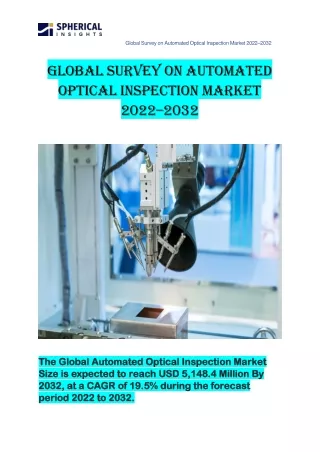
Global Optical Patterned Wafer Inspection Equipment Market Trends, Analysis, And Forecasts To 2025 Amid the way toward assembling, optical patterned wafer inspection equipment supplies are utilized for the recognition of imperfections in designed wafer. Because of expanding use of semiconductor wafer in different modern sections, for example, car and purchaser gadgets among others, the interest for optical designed wafer inspection types of gear is developing. The optical designed wafer inspection types of gear involves two advances, in particular; brilliant field investigation and dim field review. The market for optical designed wafer inspection types of gear is relied upon to be driven because of mechanical headways concerning the customer gadgets section. The rise of different innovations, for example, 3D T.Vs. Savvy T.Vs and Ultra HD T.Vs is driving the development of the optical designed wafer inspection types of gear market. The interest for these T.Vs are on the ascent and a developing interest for them will undoubtedly affect the interest for optical designed wafer inspection types of gear decidedly. These variables will bring about an expanded semiconductor capital gear spending and at last the interest for optical designed wafer investigation supplies will be affected. In addition, the surge of the semiconductor business has brought about different semiconductor makers to expand their use and creation limit on fab gear. There has an expansion in the complexities identified with the semiconductor fabricating because of new plan procedures and standards. This has prompted the expansion in the thickness of deformities of semiconductor wafers which can bring about extreme harm of the wafers. Optical designed wafer assessment supplies can assist the semiconductor makers with launching new items all the more adequately and rapidly as they would help forestall surrenders in the item. In this manner, it has turned into an indispensable issue with respect to the wafer makers to execute restorative measures keeping in mind the end goal to decrease the polluting influences that can hamper the execution of the gadgets and at last prompt the dismissal of the whole wafer. The interest for a shorter semiconductor item advancement cycle is another imperative factor driving the Development Of The Optical Designed Wafer review types of gear showcase. Request For Free Sample Of The Report @ https://www.xpodenceresearch.com/Request- Sample/105709 According to late patterns it has been watched that the optical patterened wafer inspection types optical patterned wafer inspection equipment market is seeing extraordinary rivalry as more number of makers are entering the market because of the colossal potential the market offers. This serious rivalry has brought about the different sellers working in the semiconductor business to enhance the execution of the semiconductor gadgets keeping in mind the end goal to remain ahead in the opposition. The global optical patterned wafer inspection equipment market is segmented on the basis of types, application and geography. The global market is segmented on the basis of types as dark field inspection and bright field inspection. Based on applications the global market is classified as consumer electronics,
automotive and others. The global optical patterned wafer inspection equipment market is segmented based on regions as North America, Europe, Asia-Pacific, Latin America and Middle East and Africa. Obtain Details @ https://www.xpodenceresearch.com/Reports/Optical-Patterned-Wafer- Inspection-Equipment-Market Some of the major companies in the global optical patterned wafer inspection equipment market are Applied Materials, KLA Tencor, ASML Holding, Hitachi High-Technologies, Toray Engineering, JOEL Ltd. and Tokyo Seimitsu. ????? If you have any special requirements, please let us know and we will offer you the report as you want. About Us Xpodence Research have the most extensive collection of market research reports of many categories. Xpodence Research provides the best market research solution for every industry by publishing the best possible results of great market research firms worldwide. For every particular problem, there’s a particular solution, so according to the customer needs, we provide the best possible results to them from different market research organization, whether it’s a Custom Research or Syndicated Research reports because the product that wins is the one that bridges customers to the future, not the one that requires a giant leap. Every organization, whether it is related to Pharmaceuticals, Technology, Eatables, Consumable Goods and many more demands a market research results so that they can take important decisions for more productivity and better output in this swift world. Xpodence Research gives the best possible outcome, perfect forecast, analysis and insights of market research in the form of report which is beneficial for various organisations and also to the manufacturing companies in taking the best decisions for quality production. Contact Us Xpodence Research USA Office 244 , Madison Avenue New York City, NY - 10016 United States Toll Free +1- 844-445-2861 Email : sales@xpodenceresearch.com