Download
1 / 27
270 likes | 528 Views
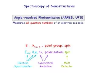
Spectroscopy of Nanostructures. Angle-resolved Photoemission (ARPES, UPS) Measures all quantum numbers of an electron in a solid. E , k x,y, z , point group, spin E kin , , , h , polarization, spin. Electron Spectrometer. Synchrotron Radiation. Mott Detector.

E N D
Spectroscopy of Nanostructures Angle-resolved Photoemission (ARPES, UPS) Measures all quantum numbers of an electron in a solid. E , kx,y, z , point group, spin Ekin , ,,h, polarization,spin Electron Spectrometer Synchrotron Radiation Mott Detector
1905 Einstein: Photoemission is a quantum effectEmax=h- 1965-1975Photoemission withsurface control Probing depth of 0.5-5nm, “nano” in one direction 1975-1985 E(k) angle-resolved, tunable synchrotron radiation 1985-1995 Empty states , inverse photoemission, pump-probe 1995-2005 Line shape with resolution < kBT Electron propagator, self-energy , lifetime 2005- … Fourier transform from k-space to real space
E(k)from Angle-resolved Photoemission E(eV) E(eV) Ni EF 3d-bands k(Å-1) 0.7 0.9 1.1 E,kmultidetection: Energy bands on TV s,p-band States withinkBTof the Fermi levelEFdetermine transport, superconductivity, magnetism, electronic phase transitions. k
Spin filter: Magnetic doping with Fe in permalloy (Ni0.9Fe0.1) shortens the lifetime of and thereby selects . Im()=Energy Width =ħ / Lifetime
Spectrometer with E,kx -Multidetection 50x50 = 2500 spectra in one scan!
Lens focused to Energy Filter Angular Multidetection
Theory Experiment EF E 0 0 kx Atom chains on a silicon surface E Spin-split band is similar to that in photoemission Sanchez-Portal et al., PRL 93, 146803 (2004) Losio et al., PRL 86, 4632 (2001)
From Reciprocal Space to Real Space Angular Pattern 1D Quantum Well States in Photoemission on a Terrace |(k)|2 (r) Phase from iterated Fourier transform cycle Mugarza et al., PR B 67, 0814014 (2003)
ky kx Imaging Molecular Orbitals by Photoemission (A) HOMO of sexiphenyl reconstructed from the 2D photoemission momentum map. (B) HOMO of an isolated sexiphenyl molecule from density functional theory (DFT). Photoemission momentum map (square root of the intensity) for sexiphenyl on Cu (110) at a binding energy of 1.9 eV which corresponds to the HOMO. Puschnig et al., Sciencexpress, 10 Sep. (2009)
Core Level Photoemission (XPS) Element selective Synchrotron radiation X-ray tube (Al K) h = 1400eV Intermediate oxidation states of Siat the Si/SiO2 interface (key to Si technology !).
Fast electrons get farther Not enough energy to excite plasmons (≈15eV) (A = 0.1 nm) Si Ge GaAs Varying the Probing Depth
X-Ray Absorption Spectroscopy (XAS, NEXAFS, XANES) • Photon energy h related to: • Core level Element • Valence orbital Bonding
Detection Modes: Electron and Fluorescence Yield Empty states • Detect the absorption of photons indirectly by looking at the decay products: • Fluorescence Yield (FY): Bulk sensitive (100-1000 nm) • Total Electron Yield (TEY): Surface sensitive (≈5nm)
Dipole selection rules: • ll1, here s p • Electric field vector E parallel to the • orientation of the molecular orbital 900 200 C-H C-C 900 200 Information about Molecular Orientation Alkanethiol self-assembled mono-layer (SAM)
* * p* Chemistry of Bio-Interfaces Double-stranded DNA • The N1sedge selects the • *-orbitals of the base pairs • All * orbitals are parallel to • the axis of the double-helix Crain et al., JAP 90, 3291 (2001)
Mean Free Path of Photons vs.Electrons in Water Path C N O 104 nm 103 nm Water Window Water Window 102 nm 10 nm 1 nm 0.1 nm 10 eV 100 eV 1000 eV Energy http://henke.lbl.gov/optical_constants/
Magnetism Catalysts Bio Environment Chemical Information from X-Ray Absorption Spectroscopy Core to Valence Transitions: 1s2p (*,*) , 2p3d, … Sharp levels (<1keV) for bond orbitals Deep levels (>1keV) for dilute species
Transition Metals: 2p3d Absorption Edge Can detect the oxidation state, spin state, and theelectric field of the ligands for one Fe atom inside a complex molecule. Fe2+ Fe3+
Time-resolved X-Ray Absorption spectroscopy These measurements provide information about spin excitations with about 100 picoseconds (ps) time resolution. To see atomic vibrations one would need <100 femtoseconds (fs) time resolution, to follow electrons in real time about 1 fs. The velocity of electrons in a metal is about 1 nm/fs at the Fermi level. X-ray absorption spectra of a solvated organic Fe complex for the low-spin ground state (blue) and an excited high-spin state (red).
Spatially Resolved X-Ray Absorption Spectroscopy Chemically resolved, but still insufficient spatial resolution Want this chemically resolved Fischer-Tropsch process for con-verting coal to liquid fuel. De Smit et al., Nature 456, 222 (2008)
PEEM and LEEM Photoemission Electron Microscope: Accelerate photoelectrons and run them through the magnifying optics of an electron microscope. Low Energy Electron Microscope: Use diffracted electrons instead.
Orientation of Nacre Platelets from PEEM with Polarized Light Oriented single crystals of CaCO3 act like bricks connected by a protein glue. Hard, but flexible to prevent cracking. Gilbert et al., JACS 130, 17519 (2008)
Scanning Tunneling Spectroscopy (STS) Atomic resolution Scanning Probe Microscopy, ed. by R. Wiesendanger, Nanoscience and Technology, Springer, Berlin 1998, ISBN 3-540-63815-6
Mapping the Density of States (DOS) by STS The density of states is given the differential conductance dI/dV: DOS Explanation: For small bias voltages («1V) and for a metallic tip the density of occupied tip states can be approximated by a step function. In an I(V) scan this tip DOS Dtip is swept past the sample DOS Dspl . Such a sweep corresponds to a convolution (represented by a star): I(E) Dtip* Dspl= Dtip(E-E’)· Dspl(E’) dE’ E = e·V The derivative of a convolution is the convolution with the derivative, and the derivative of the step function is the -function. Convolution of a function with the -function replicates this function. The result is that dI/dV is proportional to the sample DOS. The derivative is obtained by modulating the sample voltage sinusoidally and picking up the oscillating component of the current with a lock-in amplifier. Electronic noise at all other frequencies is filtered out. dI/dV I/V
Density of States from STS,Photoemission and Inverse Photoemission • The Si(111)7x7 surface (the most stable surface of silicon) has two types of broken (“dangling”) bonds: • Adatoms trade 3 broken bonds for one (yellow). • Rest atoms are part of the original truncated silicon surface (red). • An electron is transferred from adatoms to a rest atom and thereby completely fills its broken bond or-bital, producing a stable lone pair.
Magnetic Tunneling via Spin-Polarized Surface States Wave function of the spin-polarized dz2 surface state on Fe(100) and Cr(100)
Cu Mo Caveat: Sample and Tip are Involved Equally An atom jumping onto the STM tip and back reverses the contrast between Cu and Mo. Contrast reversal between Cu and Mo by changing the tunnel voltage.