Download
1 / 19
190 likes | 457 Views
NATURE | VOL 408 | 23 NOVEMBER 2000 |www.nature.com Optical gain in silicon nanocrystals. L. Pavesi*, L. Dal Negro*, C. Mazzoleni*, G. FranzoÁ² & F. Priolo² * INFM & Dipartimento di Fisica, UniversitaÁ di Trento, Via Sommarive 14, 38050 Povo, Italy

E N D
NATURE | VOL 408 | 23 NOVEMBER 2000 |www.nature.comOptical gain in silicon nanocrystals L. Pavesi*, L. Dal Negro*, C. Mazzoleni*, G. FranzoÁ² & F. Priolo² * INFM & Dipartimento di Fisica, UniversitaÁ di Trento, Via Sommarive 14, 38050 Povo, Italy ² INFM & Dipartimento di Fisica e Astronomia, UniversitaÁ di Catania, Corso Italia 57, 95129 Catania, Italy 2011. 04. 27. Kim Yeo-myung RFAD LAB, YONSEI University
CONTENTS • I. Introduction • II. Silicon nanocrystals • III. Light Amplification • IV. Gain cross-section per nanocrystal • V. Origin of gain • VI. Conclusion RFAD LAB, YONSEI University
Introduction • Light emission from silicon at R.T. • 1. Low-Dimensional • 2. Active impurities (such as erbium) • 3. New phases (such as iron disilicide) • Low Dimensional Silicon system are being actively investigated as a means of improving the light-emission properties of silicon.(quantum confinement) → But, Silicon laser has remained unlikely. • To produce a silicon-based laser, we should demonstrate its light amplification or stimulated emission • Efficient free carrier absorption → reduces the net gain • Auger saturation of the luminescence intensity at high power • significant size-dependence of the radiative energies in Si nanostructures → inhomogeneous broadening and optical losses • Light Amplification using silicon, in the form of quantum dots dispersed in silicon dioxide matrix!! RFAD LAB, YONSEI University
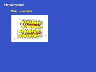
Silicon Nanocrystals • Low-dimensional silicon nanocrystalshave been produced by • 1. Negative ion implantation into ultra-pure quartz substrates • 2. Into thermally grown silicon dioxide layers on Si substrates, followed by high-temperature thermal annealing.
Silicon Nanocrystals • Absorbance and luminescence spectra at R.T for quartz sub. • A single wide emission band peaked at 800 nm • characteristic of the radiative recombination of carriers in Si nanocrystals • The rising edge is due to absorption in the quantum confined states of the nanocrystals • the peculiar feature of the near-infrared absorption band is caused by a Si.Ointerface state • Interface state : interface between Si nanocrystalsand SiO2 matrix • Microscopic nature of these interface states is still under debate • We note the spectral coincidence of the emission band and the interface state absorption band, suggesting that radiative emission in Si nanocrystalsoccurs through a radiative state associated with the nanocrystal-oxide interface
Silicon Nanocrystals • Figure 3(suplement): Electric field profile for the fundamental TE mode of a four layers waveguide at a wavelength of 0.8 μm. The waveguide was formed by a 0.1 μm thick NS layer on top of a quartz substrate and capped by a 0.06 μm thick SiO2 layer. The external medium was air. The effective refractive index of the NS implanted region, for the full line plot, was estimated by using the Maxwell Garnett approximation , which is valid for spherical particles of dielectric constant e (here we use e =15.21 as for Si) embedded in a medium of dielectric constant e M (here we use e M =2.102 as for SiO2) with a volumetric fraction f=0.28 (corresponding to Si nanocrystals with a diameter of 3 nm and a density of 2x1019 cm-3)and yielded an effective dielectric constant=3.57. Then =1.89. For the dotted line, we used an effective refractive index for the NS layer of 1.71 which was measured by ellipsometry on PE-CVD deposited NS. The profile of the refractive indexes of the two resulting structures is also shown. The optical filling factor of the mode is defined as G.
Light Amplification Modal Gain: which is the material gain adjusted to take into account the poor overlap that always exists between the optical mode and the electron envelope function in the quantum well • Veriable strip length method : to measure light amplification The sample is optically excited by a doubled Ti:sapphire laser beam (ʎ=390 nm, 2-ps pulse width, 82-MHz repetition rate) in a stripe-like geometry with variable length (l) The amplified spontaneous emission intensity IASE that is emitted from the sample edge (observation angle = 0) is measured as a function of l By assuming a one-dimensional amplifier model, IASE can be related to g by (Modal gain)
Light Amplification • At L < 0.05 cm, • Exponential increase of IASE is observed that indicates the occurrence of amplified spontaneous emission. • At L > 0.05 cm, • IASE saturates as expected for any finite power supply amplification mechanism • At low power density, we measured absorption • when the pump power was increased, the peak net modal gain increased and then saturated at values of about 100 cm-1
Light Amplification • Gain spectrum of measuring the amplified signal for various wavelengths spectrally overlaps the wavelength range of the luminescence → demonstrating that amplification is produced by the radiativestate associated with the nanocrystal-oxide interface both samples yielded similar shapes and values for the gain curve
Light Amplification • Amplified spontaneous emission spectra of sample A for different measurement conditions.
Light Amplification • Direct evidence of light amplification from our systems was provided by pump and probe transmission measurements In the presence (absence) of the pump beam the probe beam is amplified (absorbed) (population inversion) This is the first evidence of light amplification in transmission, usually named single-pass gain, in Si-based systems They are high enough to compare with those of self-assembled quantum dots made of III-V semiconductors
Gain cross-section per nanocrystal • To compare gain cross-section per nanocrystalwith the photon absorption cross-section per nanocrystal. gain cross-section per nanocrystal = 5 X 10-16 cm2 absorption cross-section per nanocrystal = 3 X 10-16cm2 Another issue concerns the comparison of the gain cross-sections that are derived from the modal and the material gain. Modal gain = 5 X 10-16 cm2 Material gain = 3 X 10-16cm2
Origin of gain • Three level model to explain the observed gain Third-level : Due to the radiative interface state observed in absorption and responsible for the luminescence emission band at 800 nm Electrons from the LUMO relax very rapidly to the interface state. Electrons in the interface state have long lifetimes
Conclusion • Modal and net material optical gains have been observed unambiguously in Si nanocrystals. • Quantitative estimates of gain crosssection per nanocrystalare orders of magnitude lower than those found in III-V semiconductor quantum dots. • However, owing to the much higher stacking density of Si nanocrystalswith respect to direct-bandgap quantum dots, similar values for the material gain are observed. • These findings open a route towards the realization of a silicon-based laser. RFAD LAB, YONSEI University
참조 • Quantum dot • From Wikipedia, the free encyclopedia • A quantum dot is a semiconductor whose excitons are confined in all three spatial dimensions. Consequently, such materials have electronic properties intermediate between those of bulk semiconductors and those of discrete molecules.[1][2][3] They were discovered at the beginning of the 1980s by Alexei Ekimov[4] in a glass matrix and by Louis E. Brus in colloidal solutions. The term "quantum dot" was coined by Mark Reed. • Researchers have studied quantum dots in transistors, solar cells, LEDs, and diode lasers. They have also investigated quantum dots as agents for medical imaging and hope to use them as qubits. • Stated simply, quantum dots are semiconductors whose electronic characteristics are closely related to the size and shape of the individual crystal. Generally, the smaller the size of the crystal, the larger the band gap, the greater the difference in energy between the highest valence band and the lowest conduction band becomes, therefore more energy is needed to excite the dot, and concurrently, more energy is released when the crystal returns to its resting state. For example, in fluorescent dye applications, this equates to higher frequencies of light emitted after excitation of the dot as the crystal size grows smaller, resulting in a color shift from red to blue in the light emitted. In addition to such tuning, a main advantage with quantum dots is that, because of the high level of control possible over the size of the crystals produced, it is possible to have very precise control over the conductive properties of the material.[5] Quantum dots of different sizes can be assembled into a gradient multi-layer nanofilm.
참조 • Quantum confinement in semiconductors • Main article: Potential well • In an unconfined (bulk) semiconductor, an electron-hole pair is typically bound within a characteristic length, called the excitonBohr radius. This is estimated by replacing the positively charged atomic core with the hole in the Bohr formula. If the electron and hole are constrained further, then properties of the semiconductor change. For example, the absorption and emission wavelength of light shifts towards smaller wavelengths.[6] This effect is a form of quantum confinement, and it is a key feature in many emerging electronic structures.[7][8] • Besides confinement in all three dimensions i.e. Quantum Dot - other quantum confined semiconductors include: • quantum wires, which confine electrons or holes in two spatial dimensions and allow free propagation in the third. • quantum wells, which confine electrons or holes in one dimension and allow free propagation in two dimensions. • Radiative recombination • Radiative recombination is the process by which an ion in state-i binds an electron from the electron sea to produce state-(i-1) with the subsequent radiation of photons. Both continuum and line photons can be produced in such a recombination event as the electron passes from the continuum (i.e. free) levels into the upper bound levels of the ion and then cascades down to form a ground state ion.
참조 • Nanocrystal • From Wikipedia, the free encyclopedia • Fahlman, B. D. has described a nanocrystal as any nanomaterial with at least one dimension ≤ 100nm and that is singlecrystalline.[1] More properly, any material with a dimension of less than 1 micrometre, i.e., 1000 nanometers, should be referred to as a nanoparticle, not a nanocrystal. For example, any particle which exhibits regions of crystallinity should be termed nanoparticle or nanocluster based on dimensions. These materials are of huge technological interest since many of their electrical and thermodynamic properties show strong size dependence and can therefore be controlled through careful manufacturing processes. • Crystalline nanoparticles are also of interest because they often provide single-domain crystalline systems that can be studied to provide information that can help explain the behaviour of macroscopic samples of similar materials, without the complicating presence of grain boundaries and other defects. Semiconductornanocrystals in the sub-10nm size range are often referred to as quantum dots. • Crystalline nanoparticles made with zeolite are used as a filter to turn crude oil onto diesel fuel at an ExxonMobil oil refinery in Louisiana, a method cheaper than the conventional way. • A layer of crystalline nanoparticles is used in a new type of solar panel named SolarPly made by Nanosolar. It is cheaper than other solar panels, more flexible, and claims 12% efficiency. (Conventionally inexpensive organic solar panels convert 9% of the sun's energy into electricity.) Crystal tetrapods 40 nanometers wide convert photons into electricity, but only have 3% efficiency. (Source: National Geographic June 2006) • The term NanoCrystal is a registered trademark[2] of ElanPharma International Limited (Ireland) used in relation to Elan’s proprietary milling process and nanoparticulate drug formulations.
참조 • Inhomogeneous Broadening • Inhomogeneous broadening is an increase of the Linewidth of an atomic transition caused by effects which act differently on different radiating or absorbing atoms. This can be caused e.g. by the different velocities of the atoms of a gas, or by different lattice locations of atoms in a solid medium. Inhomogeneous broadening is strongly related to Inhomogeneous Saturation in LaserGain media. • Tansmissionelectron microscopy • From Wikipedia, the free encyclopedia • Transmission electron microscopy (TEM) is a microscopy technique whereby a beam of electrons is transmitted through an ultra thin specimen, interacting with the specimen as it passes through. An image is formed from the interaction of the electrons transmitted through the specimen; the image is magnified and focused onto an imaging device, such as a fluorescent screen, on a layer of photographic film, or to be detected by a sensor such as a CCD camera.
참조 • Definition of Gain • Optical Gain: In terms of the difference between the stimulated emission and absorption rates. • Modal Gain: which is the material gain adjusted to take into account the poor overlap that always exists between the optical mode and the electron envelope function in the quantum well. (I.e: modal gain=material gain* confinement factor) • Differential gain: The rate at which gain increases as we inject more carriers, dg/dN.