IV. Conclusion
A 1V Full-band Cascoded UWB LNA with Resistive Feedback Ruey-Lue Wang 1 , Min-Chuan Lin 2 , Chih-Cheng Lin 2 , Cheng-Fu Yang 3. 1 Department of Microelectronic Engineering, National Kaohsiung Marine University, No. 142, Hai-Chuan Rd. Nan-Tzu, Kaohsiung, Taiwan, ROC

IV. Conclusion
E N D
Presentation Transcript
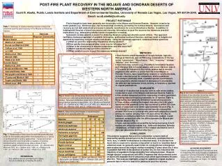
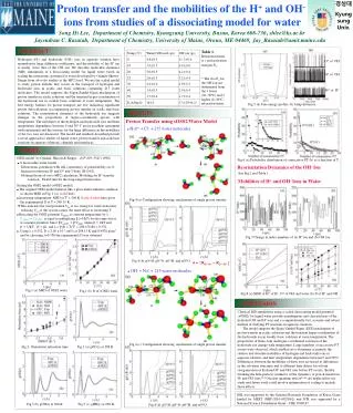
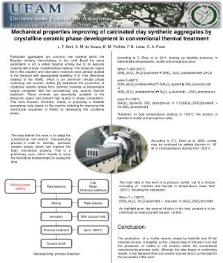
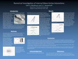
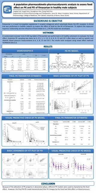
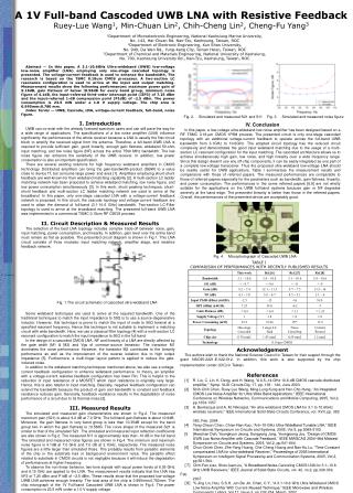
A 1V Full-band Cascoded UWB LNA with Resistive Feedback Ruey-Lue Wang1, Min-Chuan Lin2, Chih-Cheng Lin2, Cheng-Fu Yang3 1Department of Microelectronic Engineering, National Kaohsiung Marine University, No. 142, Hai-Chuan Rd. Nan-Tzu, Kaohsiung, Taiwan, ROC 2Department of Electronic Engineering, Kun Shan University, No. 949, Da Wan Rd., Yung-Kang City, Tainan Hsien, Taiwan, ROC 3Department of Chemical and Materials Engineering, National University of Kaohsiung, No. 700, Kaohsiung University Rd., Nan-Tzu, Kaohsiung, Taiwan, ROC IV. Conclusion In this paper, a low-voltage ultra-wideband low-noise amplifier has been designed based on a RF TSMC 0.18-μm CMOS 1P6M process. The presented circuit is only one-stage cascoded topology with an additional voltage-current feedback to operate across the full-band UWB bandwidth from 3.1GHz to 10.6GHz. The adopted circuit topology has the reduced circuit complexity and demonstrates the good input wideband matching due to the usage of a multi-section LC resonant configuration for the input matching. The cascoded architecture allows us to achieve simultaneously high gain, low noise, and high linearity over a wide frequency range. Since this design doesn’t use any off-chip components, it can be easily integrated as one part of a complete low-voltage transceiver. Thus the proposed ultra-wideband low-voltage LNA should be readily useful for UWB applications. Table I summarizes the measurement results and comparisons with those of referred papers. The measured performances are comparable to those of referred papers especially for the parameters such as bandwidth, gain flatness, linearity, and power consumption. The performances in the some referred papers [6,8] are not wholly suitable for the applications on the UWB full-band systems because gain or NF degrades severely at the band edge. The presented linearity is better than those in the referred papers. Overall, the performances of the presented device are acceptably good. Acknowledgement The authors wish to thank the National Science Council in Taiwan for their support through the grant NSC95-2221-E-022-012. In addition, this work is also supported by the chip implementation center (CIC) in Taiwan. References [1] R. Liu, C. Lin, K. Deng, and H. Wang, "A 0.5–14-GHz 10.6-dB CMOS cascode distributed amplifier," Symp. VLSI Circuits Dig. 17, pp. 139 - 140, June 2003. [2] Shih-Chih Chen, Ruey-Lue Wang, Ming-Lung Kung and Hen-Cho Hung, “An Integrated CMOS Low Noise Amplifier for Ultra Wide Band Applications,” IEEE International Conference on Wireless Networks, Communications and Mobile Computing, 2005, Vol.2, pp.1354-1357. [3] A. Bevilacqua and A. M. Niknejad, "An ultra-wideband CMOS LNA for 3.1 to 10.6GHz wireless receivers," IEEE International Solid-State Circuits Conference, vol. XVII, pp. 382 - 383, Feb. 2004. [4] Yang-Chaun Chen, Chien-Nan Kuo, “A 6~10-GHz Ultra-WideBand Tunable LNA,” IEEE International Symposium on Circuits and Systems, 2005, Vol.5, pp.5099-5102. [5 ]Heechan Doh, Youngkyun Jeong, Sungyong Jung, Youngjoong Joo, “Design of CMOS UWB Low Noise Amplifier with Cascode Feedback,” IEEE MWSCAS 2004−Mid Midwest Symposium on Circuits and Systems, 2004, Vol.2, pp.641-644. [6] Chun-Chieh Chen, Zhe-Yang Huang, Che-Cheng Huang and Nan-Ku Lu, “Time-Constant compensated LNA for ultra-wideband Receiver,” Proceedings of 2005 International Symposium on Intelligent Signal Processing and Communication Systems, 2005, Vol.2, pp.561-564. [7]Chih-Fan Liao, Shen-Iuan Liu, “A Broadband Noise-Canceling CMOS LNA for 3.1–10.6 GHz UWB Receivers,” IEEE Journal of Solid-State Circuits, vol. 42, no.2, pp.329-339, Feb. 2007. [8] Yi-Jing Lin, Hsu, S.S.H, Jun-De Jin, Chan, C.Y., “A 3.1-10.6 GHz Ultra-Wideband CMOS Low Noise Amplifier With Current-Reused Technique,” IEEE Microwave and Wireless Components Letters, Vol.17, Issue 3, pp.232-234, March, 2007. IEEE RFIT 2007 Abstract— In this paper, A 3.1-10.6GHz Ultra-wideband (UWB) low-voltage low-noise amplifier (LNA) employing only one–stage cascoded topology is presented. The voltage-current feedback is used to enhance the bandwidth. The research is based on the TSMC 0.18um CMOS processes. A two-section LC resonance configuration is used to arrive at the input and output matching. Measurement results show the following performances: maximum power gain of 9.18dB, gain flatness of below ±0.58dB for every band group, minimum noise figure of 4.1dB, the input-referred third-order intercept point (IIP3) of 7.25 dBm and the input-referred 1-dB compression point (P1dB) of –2.5 dBm. The power consumption is 23.5 mW under a 1.0 V supply voltage. The chip area is 0.995mm×0.780 mm. Index Terms— UWB, Cascode, LNA, voltage-current feedback, full-band, noise figure. I. Introduction UWB can co-exist with the already licensed spectrum users and can still pave the way for a wide range of applications. The specifications of a low noise amplifier (LNA) influence significantly the performances of the whole receiver because a LNA is usually the first circuit block to amplify the received signal from the antenna. Therefore, a full-band UWB LNA is required to provide sufficient gain, good linearity, enough gain flatness, wideband 50-ohm input matching, and low noise figure (NF) across the entire 7500 MHz bandwidth. The low noise figure can enhance the sensitivity of the UWB receiver. In addition, low power consumption is also an important specification. There are several existing solutions for high frequency wideband amplifiers in CMOS technology. Distributed amplifiers can bring the gain-bandwidth-product (GBW) to a value close to device fT, but consume large power and area [1]. Amplifiers employing shunt-shunt feedback are well-known for their wideband matching capability [2]. A multi-section LC ladder matching network has been proposed to achieve wideband matching, low noise figure, and low power consumption simultaneously [3]. In this work, shunt peaking techniques, shunt-shunt feedback and multi-section LC ladder matching network are used to arrive at the broadband. In this paper, only one-stage cascoded LNA with a voltage-current feedback network is proposed. In this circuit, the cascode topology and voltage-current feedback are used to attain the demand of full-band (3.1-10.6 GHz) bandwidth. Two-section LC-Filter topology is used to arrive at the broadband matching. The presented full-band UWB LNA was implemented in a commercial TSMC 0.18um RF CMOS process. II. Circuit Description & Measured Results The selection of the best LNA topology includes complex trade-off between noise, gain, input matching, power consumption, and linearity. In addition, gain level over the entire band must remain as flat as possible. The presented circuit diagram is shown in Fig.1. This LNA circuit consists of three modules: input matching network, amplifier stage, and resistive feedback network. Some wideband techniques are used to arrive at the required bandwidth. One of the traditional techniques to match the input impedance to 50Ω is to use a source-degenerative inductor. However, this technique is prone to match the input of node to 50Ω teminal at a specified resonant frequency. Hence this technique is not suitable to implement a matching circuit with wide bandwidth. Here, we use a classical filter topology [4] with a multi-section LC resonant configuration to match the input impedance to 50Ω in the full band. In the design of a cascoded CMOS LNA, NF and linearity of a LNA are directly affected by the gate width (M1 & M2) and Vgs of common-source transistor. The transistor M1 dominates the noise performance. However, the transistor M2 contributes to the linearity performance as well as the improvement of the reverse isolation due to high output impedance [5]. Furthermore, a multi-finger layout pattern is applied to reduce the gate-induced noise. In addition to the wideband matching techniques mentioned above, we also use a voltage-current feedback configuration to enhance wideband performance. In theory, an amplifier with a voltage-current resistive feedback configuration has lower Rin. This is helpful to the reduction of input resistance of a MOSFET which input resistance is originally very large. Hence, this is also helpful to input matching. Basically, negative feedback configuration can extend the bandwidth because the product of gain and bandwidth is constant and feedback resistance reduces gain. Generally, feedback resistance results in the degradation of noise performance of a circuit due to its thermal noise [2]. III. Measured Results The simulated and measured gain characteristics are shown in Fig.2. The measured maximum gain (S21) is about 9.2 dB at 7.0 GHz. The full-band gain flatness is about ±0.9dB. Moreover, the gain flatness in very band group is less than ±0.35dB except for the band group two in which the gain flatness is ±0.58dB. The curve shape of the measured S21 is similar to that of the simulated S21. The simulated and measured input reflection coefficients are also shown in Fig.2. The measured S11 is approximately less than -10 dB in the full band. The simulated and measured noise figures are shown in Fig.4. The minimum and maximum noise figure is 4.1dB at 7.0 GHz and 7.0 dB at 3.1GHz, respectively. The measured noise figures are a little larger than simulated those. This probably results from parasitic elements of the chip or the substrate loss or background environment noise. The parasitic effect related to substrate in CMOS circuits is not negligible because it will induce the degradation of performances at higher frequency. To observe the non-linear behavior, two-tone signals with equal power levels at 6.05 GHz and 6.15 GHz are applied to the LNA. The measurement results indicate that the LNA has IIP3 of 7.25 dBm and P1dB of –2,5 dBm. These results show that the proposed low-voltage UWB LNA achieves enough linearity. The total area of the chip is 0.995mm×0.780mm. The chip micrograph of the 1V Full-band Cascoded UWB LNA is shown in Fig.4. The power consumption is 23.5 mW under a 1.0 V supply voltage. Fig. 2. Simulated and measured S21 and S11 Fig. 3. Simulated and measured noise figure TABLE I COMPARISON OF PERFROMANCES WITH RECENTLY PUBLISHED RESULTS Fig. 4. Microphotograph of Cascoded UWB LNA TABLE I COMPARISON OF PERFROMANCES WITH RECENTLY PUBLISHED RESULTS IV. Conclusion Fig. 1.The circuit schematic of cascoded ultra-wideband LNA