Download
1 / 11
180 likes | 795 Views
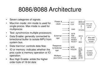
Lecture 12 8086/8088 Hardware Specifications and Memory Interface. Presented By Dr. Shazzad Hosain Asst. Prof. EECS, NSU. 8086 Microprocessor. 8088 Microprocessor. 8.1: Barry B. Brey. Chapter 9: Memory Interface. Address Pins. 1K Memory has A 0 – A 9 4K Memory has A 0 – A 11.

E N D
Lecture 128086/8088 Hardware Specifications and Memory Interface Presented By Dr. ShazzadHosain Asst. Prof. EECS, NSU
8086 Microprocessor 8088 Microprocessor 8.1: Barry B. Brey
Chapter 9: Memory Interface Address Pins • 1K Memory has A0 – A9 • 4K Memory has A0 – A11 Output/Data Pins • O0 – O7 for 8 bit computer • O0 – O15 for 16 bit computer
Address Decoding • Why need address decoding? • 8086/8088 has 20 address pins • But EPROM, the memory device has less space • For example, 2716 EPROM is a 2K memory device
NAND Gate Decoder 1111 1111 1000 0000 0000 = FF800H 1111 1111 1111 1111 1111 = FFFFFH • Decode memory address locations FF800H – FFFFFH Figure: 9-12
More Example • Develop a NAND gate decoder so that it decodes the memory range DF800H – DFFFFH
Develop a 64K memory bank using eight 2764 EPROMs, where each 2764 EPROM is a 8K memory device and it address the memory locations F0000H – FFFFFH 0000 0000 0000 0000 = F0000H 1111 0001 1111 1111 1111 = F1FFFH 0010 0000 0000 0000 = F2000H 1111 0011 1111 1111 1111 = F3FFFH 0100 0000 0000 0000 = F4000H 1111 0101 1111 1111 1111 = F5FFFH 0110 0000 0000 0000 = F6000H 1111 0111 1111 1111 1111 = F7FFFH 1000 0000 0000 0000 = F8000H 1111 1001 1111 1111 1111 = F9FFFH 1110 0000 0000 0000 = FE000H 1111 1111 1111 1111 1111 = FFFFFH * *
0000 0000 0000 0000 = F0000H 1111 0001 1111 1111 1111 = F1FFFH 0010 0000 0000 0000 = F2000H 1111 0011 1111 1111 1111 = F3FFFH 0100 0000 0000 0000 = F4000H 1111 0101 1111 1111 1111 = F5FFFH 0110 0000 0000 0000 = F6000H 1111 0111 1111 1111 1111 = F7FFFH 1000 0000 0000 0000 = F8000H 1111 1001 1111 1111 1111 = F9FFFH 1110 0000 0000 0000 = FE000H 1111 1111 1111 1111 1111 = FFFFFH * *
A13 A14 A15 A16 A17 A18 A19
References • Chapter 8, 9 The Intel Microprocessors – by Barry B. Brey
![8086 [2]](https://cdn1.slideserve.com/2457127/8086-2-dt.jpg)