Download

1 / 11
110 likes | 193 Views
WireGrid electronics in the Linac 4 tunnel. Technology Choice. At the time of designing the radiation levels were unknown. Relatively little time for development. No choice was given about where to place the equipment.

E N D
WireGrid electronics in the Linac 4 tunnel Gerrit Jan Focker, BE/BI/PM
Technology Choice. • At the time of designing the radiation levels were unknown. • Relatively little time for development. • No choice was given about where to place the equipment. • To reach the specifications the electronics should be near the detectors (Initially 1m80, new design would allow ~8m). • Therefore we have opted for a system with only the absolutely necessary electronics near the beamline: • Only amplifiers, • No logic, • Remote power supplies. Gerrit Jan Focker, BE/BI/PM
Grid overview. • Between Grid and Amplifier: two cables with twisted pairs with individualscreening. The two cables will be mounted together in large Harting 72-pin connectors. • Between Amplifiers and Controls a single cable is proposed (CERN ND100) mounted with Harting 108-pin connectors. • Power and I/O control are handled by the same ND100 cables, no additional cabling is foreseen. • Bias +120V directly onto measuring wires. Gerrit Jan Focker, BE/BI/PM
Amplifier-boxes • Up to 32 channels per box. • Motherboard with daughter-boards carrying 4 amplifiers each. • Amplifiers with BW = ~1MHz, • Input amplifiers can be biased up to +120V. Gerrit Jan Focker, BE/BI/PM
Linac4 Amplifier (1) Gerrit Jan Focker, BE/BI/PM
Linac4 Amplifier (2). Gerrit Jan Focker, BE/BI/PM
Design Details (1). • Amplifier’s Maximum Electrical Input: 10mA, • Amplifier’s highest sensitivity: 1μA full scale, • The calculated input-related noise-level is ~2nA at 1MHz BW. • With software amplification highest sensitivity will be (=<)200nA full scale. • Overall BW is defined by the cable-length between grid and electronics, • The newer design allows longer cables (8m). • Isolated input-stage: Bias of up to +120V on measuring wires. • The design foresees to use test-resistances: • At the grid in the vacuum-chamber, • Outside the vacuum-chamber at the cable-connection, • At the amplifier-inputs. • The design is made to accept different types of amplifiers so it can be used for other machines as well. Gerrit Jan Focker, BE/BI/PM
Design Details (2). • No electronic switches: miniature reed-relays. • The amplifiers cannot consume too much power, • Cable-length, noise-level and lifetime. • Input-protection by small-signal diodes BAV199 and one small zener-diode BZX84C3,3. • Amplifiers AD8610ARZ, AD8032ARZ and AD8397ARZ, • All from Analog Devices XFCB process, • Not that much choice anyway… • Report from the European Space Agency and NASA: • “Commercial Components Identification In Naturally Radiation Hardened Technologies” 2002ESASP.507...17M • They have tested chips from this family which were still o.k. after 100kRad(Si) radiation. • These chips appear not to suffer from single event upset. Gerrit Jan Focker, BE/BI/PM
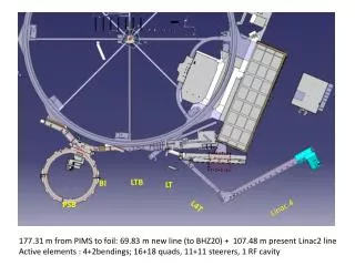
Place in the tunnel. Gerrit Jan Focker, BE/BI/PM
Place in the tunnel. Gerrit Jan Focker, BE/BI/PM
Our goal of this meeting. • At the place of our rack we had expected more radiation due to the bend in the beam and especially due to the beam dump. • Our questions: • Is it useful to have screening around our electronics? • If yes, what could this screening consist of? • Do the experts have any idea about the lifetime of our electronics? Gerrit Jan Focker, BE/BI/PM