Download
1 / 15
150 likes | 255 Views
This project focuses on the quality control system for MPG readout planes through Time Domain Reflectometer (TDR) technique. Topics include the KLOE-2 Inner Tracker upgrade, anodic sheet design, XV readout layout, signal reflection on transmission lines, TDR test methodology, and TDC implementation in Spartan3 FPGA. The system ensures data integrity and accuracy through DNL and INL characterization and prototypes like TDR on coaxial cables. The TDC delay line characterization improves performance using Statistical Code Method for precise measurements.

E N D
A quality control system for the integrity check of MPGD readout planes exploiting TDR technique by G. Fanizzi on behalf of KLOE-2 I.T. group
Summary • The KLOE-2 Inner Tracker - readout geometry • A quality assurance test setup • Time Domain Reflectometer Method • FPGA implementation and features • Preliminary test • Characterization: DNL and INL by SCM • Test results on KLOE2 IT anode • Conclusions 2
KLOE-2 InnerTracker up-grade • 4 independent tracking layers for a fine vertex reconstruction of KS and η • 200 µm σrφ and 500 µm σZspatial resolutions with XV readout • 700 mm active length • from 130 to 220 mm radii • 1.8% X0 total radiation length in the active region • Realized with Cylindrical-GEM detectors 3
Anodic sheet for KLOE-2 I.T. X pitch 650 µm V pitch 650 µm 1000 µm • Distinguishing XV readout designed for the cylindrical geometry • X Strips on a layer for r-φ coordinate • V Strips at 40° formed by Pads connected by internal vias (220.000 VIAs!) • Crossing of X and V gives Z coordinate 40° Schematic of XV strips-pads geometry top-view (above) and cross-section (below). On the left a picture of the anode plane. Manufactured by EST-DEM CERN x x V I A Ka Ka+glue Cover lay 4
The Anode is shared out in a 2 dimensions layout having a XV geometry, X and V strips read out is shared out at both ends. Rotated by roughly 40°, such strip’s net provides 2D positioning for the particle passing through the layer. Plugged to only one access of the strips, we perform Test on the reflected signal in order to verify strip integrity Test of short circuits between all strips and pads IT Read Out Layout 5
Signal reflection on transmission lines Reflectometer methods and test devices are commonly used since signal cable: the length of the transmission line and hence a possible damage in it is evaluated by measuring the delay of reflectedsignal. In the picture above: reflections produced by resistive terminations R at one end of a transmission line; Z0 is the characteristic impedance of the line. HEWLETT-PACKARD JOURNAL Tech infos of HP laboratories vol.15 no.6 (Feb. 1964) 1-8. 6
TDR test exploits time measure -> TDC The drawing shows the foreseen run of a signal, in this case a transition from high to low state, injected into an un-terminated transmission line. The first edge occurs when the signal is injected at the input while the second edge is observed after that the signal reflected comes back (in red a threshold level) . V input V input delay = 2 l / v Input/Output pad of the FPGA Time of injection time 7
TDC by Tapped Delay Lines Few examples of TDC by delay lines in ASIC: HP5371A Stephenson, 1989 Resolution 200 ps 0.8 μm CMOS Gorbics et al., 1997 Resolution 46.9 ps 0.25 μm CMOS Mota et al., 2000 Resolution 24.4 ps 0.6 μm CMOS Mantyniemi et al., 2002 Resolution 29.6 ps 0.35 μm CMOS Jansson et al., 2006 Resolution 12.5 ps Left schematics from J.Kalitz in Metrologia 41 (2004) 17–32 “Review of methods for time interval measurements with picosecond resolution” 8
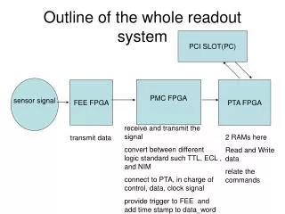
TDCimplemented in a Spartan3 FPGACLBasdelayunit • We have designed a circuit to check the strips integrity by measuring the timing of reflected signals. We have implemented the digital time conversion in a FPGA (clock @ 250MHz) by using the single CLB as delay element and register. Moreover all encoding and control logic have been implemented in the same FPGA : • A course counter with 4 ns resolution • Fine counter by delay lines with time resolution 100 ps • Circuit implementation based on a single FPGA (Xilinx_XC3s400): • Simple and robust • Off-the-shelf component • Cost-effective 9
TDR prototype: a qualitative trial on a coaxial cable A preparatory test has been performed on a coaxial cable (LEMO type C-50-2-1) cut onwards in steps of roughly 1 cm Calculated Delay (ns) => y Length of cable (cm) => x y = 0,102 x + 55 r² = 0,9994 Max residual = 157 ps RMSD = 64 ps root-mean-square deviation or rms of residual 10
TDC delay line characterization:DNL and INL by SCM Statistical Code Method J.Kalitz in Metrologia (2004) above-cited and various Appl. Notes by Maxim, Analog Devices. DNLi = (ni– nth) / nth INLi = Σ DNLi / M Ntot is the total amount of events collected; M is the number of bins; nth is the expected number of events per bin (ideally would be equal to Ntot / M ); ni is the amount of collected events per bin. Data with radiative source 90Sr Coincidences by two Scintillators DNL and INL calculated by SCM DNL and INL within 1 LSB Note 1: results validated by other sources (external pulse generator and cosmic rays). Note 2: results from raw data without processing. 11
TDR: a test setupfor IT Anode Main features: Compact + Cost-effective. Software for Test quick and automatic. Interface with an external PC by RS232 and/or Ethernet. One board can check up to 120 chs (one plug). Several boards can be fitted together in order to test an huge number of channels Modularity. Easy programming/debugging/upgrading the device via Firmware Versatile. 12
First case of study:KLOE-2 IT Layer 2 anodic sheets X strips sheet 1 Summary of defects found on four samples of the readout anode plane for the Layer 2 of the cyl.GEM IT for KLOE-2. Vleft strips sheet 1 Vright strips sheet 1 open channel = 475 13
Second case of study:Sheet num.2 for Layer 1 Below on the left the plot of calculated delay for the X strips of Layer 1 - Sheet2 Below on the right the detail of the 4th plug (test board n.3) Defects found on a sample (named sheet 2) of the readout anode plane for the Layer 1 14
Conclusions • A very reliable quality assurance system for the readout plane of MPGD has been developed. • Test system outlines: • Time Domain Reflectometer Method • Easy implemented in basic FPGA(stock availability, cost-effective) • Software for analysis, data log via Ethernet and Auto-calibration • Modular technology (easy-fitting to different readout geometries) • Resolution 100 ± 62 ps(without calibration and processing, roughly 1 cm coax cable) • DNL and INL within 1 LSB • Test on KLOE2 IT anode planes shows benefits of the device • A test setup is available in Bari to test the readout planes of I.T. detector in KLOE apparatus. Ready to test massive production. 15