Download
1 / 9
90 likes | 303 Views
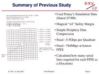
Summary of Previous Study. Used Penny’s Simulation Data (Dated 2/7/00). Magical “x4” Safety Margin. Simple Periphery Data Compression Need ~5.5Gbps per Quadrant Need ~784Mbps at hottest FPIX Calculated how many serial lines required for each FPIX as a f(location). Summary of Previous Study.

E N D
Summary of Previous Study • Used Penny’s Simulation Data (Dated 2/7/00). • Magical “x4” Safety Margin. • Simple Periphery Data Compression • Need ~5.5Gbps per Quadrant • Need ~784Mbps at hottest FPIX • Calculated how many serial lines required for each FPIX as a f(location) Pixel Readout
Summary of Previous Study Number of Serial Data Lines Required Total number of data lines required per quadrant is dominated by low occupancy chips Pixel Readout
Summary of Previous Study Pixel Readout
FPIX Readout Design Considerations • Point to Point with common CLK and Control per module. • Robust…many links in inaccessible area. • Avoid PLL/DLL…require low jitter inputs and long recovery times. • Want loose requirements for CLK & DATA jitter • Ability to control and readout directly from FPGA (flexibility and cost) Pixel Readout
Pixel Readout • Send two CLKs to each FPIX module • CLKA & CLKB are of same frequency but 90deg out of phase. Pixel Readout
FPIX Block Pixel Readout
Clock Recovery @ FPIX • 50% duty cycle recovered CLK if CLKA & CLKB are 90deg out of phase. • Easier to implement than edge detect with fixed delay. • Allows for scaling of readout frequency (replace XTAL on Readout Board) while maintaining 50% duty cycle. Pixel Readout
DATA/CLK Alignment • No delay elements required for CLK/DATA alignment. • Alignment scales properly with frequency. Pixel Readout
At the Receiver FPGA • FF in Virtex-E FPGA have very fast Setup (340ps) & Hold (0ps) allowing for large noise margin in CLK/DATA alignment. • No Global routing resources required, so receiving multiple chips per FPGA is possible. Pixel Readout