Download
1 / 5
50 likes | 64 Views
The effectiveness and working capability of any manufactured product hugely depend on the PCB design services as they provide the physical platform for designing the complete unit. For this, the engineer responsible for it must be fully aware of the multiple consideration factors of the related components and designs.<br><br>View more: https://www.greatpcb.com/pcb-assembly/

E N D
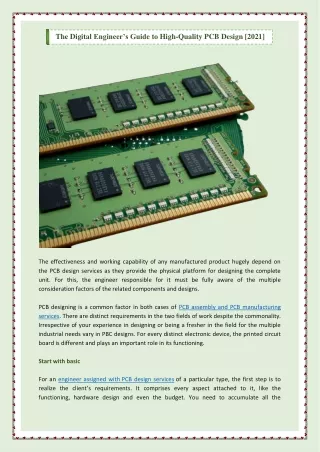
The Digital Engineer’s Guide to High-Quality PCB Design [2021] The effectiveness and working capability of any manufactured product hugely depend on the PCB design services as they provide the physical platform for designing the complete unit. For this, the engineer responsible for it must be fully aware of the multiple consideration factors of the related components and designs. PCB designing is a common factor in both cases of PCB assembly and PCB manufacturing services. There are distinct requirements in the two fields of work despite the commonality. Irrespective of your experience in designing or being a fresher in the field for the multiple industrial needs vary in PBC designs. For every distinct electronic device, the printed circuit board is different and plays an important role in its functioning. Start with basic For an engineer assigned with PCB design services of a particular type, the first step is to realize the client’s requirements. It comprises every aspect attached to it, like the functioning, hardware design and even the budget. You need to accumulate all the
requirements after analyzing the project and present them with the unit that can fit their pocket. Also, ensure the following at the beginning for wastage of resources Operating environment Power supply options Communication mechanisms Understand the representation After you are over with analyzing the project necessities, the real process begins. Representing the design's blueprint, called the schematic diagram, is the major step for engineers in PCB design services. The schematics control the accuracy and completeness of the project's success, including the essential designing details like PINs, names, component values, ratings, etc. In simple words, it represents the connections between the components in a symbolic way. It is crucial to make it at the start to check potential problems and review their performance.
Bill management It would be best if you simultaneously generated bills of materials while creating the schematics as it is a good professional practice. Analyze the maximum operating voltages and current levels of each circuit segment to determine the critical components. Evaluating these tolerating criteria, you can reconsider the components as per budget, availability or client’s preference. Keep it up-to-date as the BOM comprises quantities, reference designators, distinct values, part numbers of manufacturing and footprints for each component involved. Additionally, provide essential details for explanatory and estimation purposes. Correct component placement The most crucial part is to place the right components at the right nodes of the circuit or the whole functioning hampers. Wrong placement can cause multiple issues like noise issues, thermal problems, power imbalance and many more. Each component has distinct importance so identify their use and correct location. However, the most common order of their placing followed by designers is:
1.Connectors 2.Power circuits 3.Sensitive and precision circuits 4.Critical circuit components 5.All other elements You need to review the specific aspects of your design to place rightly and adjust the above setting. Address the constraints Only designing will not serve the purpose successfully; you need to take care of the various troubling factors and consider their resolving ways. The three most common management areas are thermal conditions, mechanical constraints and power controlling. Thermal issues result in poor performance, hence placing thermocouples in critical nodes are vital. Mechanical and power constraints can get resolved by analyzing the hardware embedded design and abiding by the regulatory guidelines while making schematics. Final words Last but not the least, remember to evaluate the quality of your design and its components. It is better to conduct a DFM and DFT checklist review before signing off to generating Gerber files. It verifies the correct placements, routing ways, scan the thermal integrities and signalling. Always remember the basic discussed aspects to design a well-functioning and cost-effective PCB, qualifying industrial standards.
CONTACT US CONTACT US Address: 22, Science Park, The Northern part of HeYi Village, ShaJing Town, Bao An, Shenzhen, GuangDong, China, 518104 Phone: +86-755-27810810 Fax: +86-755-27810813 Email: sales@greatpcb.com WhatsApp: +86-13682523810 Skype: GREATPCB Website: http://www.greatpcb.com