
MIMOSA V: High-Precision Pixel Chip Detector Technology
E N D
Presentation Transcript
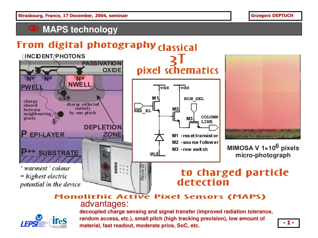
MAPS technology advantages: decoupled charge sensing and signal transfer (improved radiation tolerance, random access, etc.), small pitch (high tracking precision), low amount of material, fast readout, moderate price, SoC, etc.
MIMOSA V 1×106 pixel device • Chip-Detector design 3T design • 0.6 µm CMOS process with 14 µm epitaxial layer, • 4 matrices of 512 × 512 pixels read-out in parallel; pixel: 17 × 17 µm2, diodes: P1 - 9.6 pm2, P2 - 24.0 pm2, control logic and all pads aligned along one side, results: Noise mean ENC: 20.74 e- detection efficiency MIPs (e): 99.3% spatial resolution MIPs (s): 1.7 µm pixel-pixel gain nonuiformity ~3% MIMOSA V Chip design not optimised for any particular application, aimed at relativistic charged particle detection - DESIGNED in joined IReS-LEPSI effort in 2001 MIMOSA = Minimum Ionising Particle MOSAPS
MIMOSA V 1×106 pixel device • Architecture of the prototype • Matrix of sequentially addressed pixels, multiplexed on single output buffer.
MIMOSA V 1×106 pixel device • Default Readout Method • Readout time = Integration time ~8 ms @ 40 MHz fclk.
back-side illuminated MIMOSA V - mounting • Back-side illuminated thinned M5 device – a test vehicle for demonstration of 20 keV E- detection capability for Beam Monitoring system and other affined applications • Bonding pads 85×85 µm2 inside 10 µm deep wells • positive response from microbonding sa - idea of use Au ball-bonding technique – not successful because of pad cratering • finally 17 µm Al wedge bonding with special deep wedge was used