Download
1 / 18
180 likes | 195 Views
This introduction provides an overview of a voltage controlled voltage source with high gain, including its equivalent circuit model and voltage transfer curve. It also explores the ideal operational amplifier model and fundamental amplifier configurations such as inverting and non-inverting amplifiers. The effects of finite open-loop gain and the frequency response of real op-amps are discussed.

E N D
Introduction • a voltage controlled voltage source with very high gain. • five terminals four ports active element. • In+Ip+Ic++Ic-+Io=0 Equivalent circuit model of op-amp Vi=Vp-Vn. Ri is the input resistance Ro is the output resistance Vo=AVi=A(Vp-Vn)
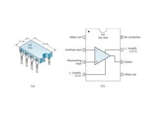
Voltage Transfer Curve In reality A, Ri are finite and Ro>0 The output is limited by power source For a 741 op-amp powered with VCC= +10V and VEE= -10V, Vo will saturate (reach the maximum output voltage range) at about ±10 V. With an A=200,000V/V saturation occurs with an input differential voltage of 10/200,000 = 50μV, a very small voltage. How to use it in circuits?
Ideal op-amp model Ideal op-amp conditions: Ip=In=0 No current into the terminals Ri=∞ Infinite input resistance Ro=0 Zero output resistance A ∞ Infinite open loop gain Ip=In=0 and Ri=∞ makes no power demands on the input signal source. Ro=0 makes the output voltage independent of the load . Even though the ideal op-amp model deviates much from the real op-amps, the ideal conditions in the ideal op-amp model are very useful in the design and analysis of circuits.
Fundamental Amplifier Configurations (a) Inverting amplifier (b) Non-inverting amplifier (c) Differential amplifier (d) Summing amplifier
Inverting Amplifier— Ideal op-amp circuit analysis Ideal op-amp conditions: Ip=In=0 No current into the terminals Ri=∞ Infinite input resistance Ro=0 Zero output resistance A ∞ Infinite open loop gain
Non-Inverting Amplifier: Ideal op-amp circuit analysis Ideal op-amp conditions: Ip=In=0 No current into the terminals Ri=∞ Infinite input resistance Ro=0 Zero output resistance A ∞ Infinite open loop gain
The Voltage Follower Purpose ?
Inverting Amplifier — Effect of Finite Open-Loop Gain The current through R1 is now Considering I1=I2, the output voltage Vo can thus be determined from
Inverting Amplifier — Effect of Finite Open-Loop Gain Let’s consider an inverting amplifier design with R1=10kΩ and R2=100kΩ. In this case, the ideal voltage gain is -10. By assuming that A ranges in values from 1,000 V/V to 10,000,000V/V, Table I shows the real gain and the resulting deviation in % from the ideal case
Non-Inverting Amplifier — Effect of Finite Open-Loop Gain Since In=Ip=0, we have I1=I2and therefore Since the voltage Vi = Vp-Vn = Vin-Vn, the output voltage is given by
Differential Amplifier: Ideal op-amp circuit analysis The output voltage is In order to obtain Vout=0 when Vin1=Vin2 only if System is linear and so we may apply superposition Which holds only if The contribution of the signal Vin2to the output is The output voltage is now The contribution of the signal Vin1 to the output is
Real Op-Amp Frequency Response Real Op amps have a frequency dependant open loop gain Where
Real Op-Amp Frequency Response If the open loop bandwidth is so small, how can the op amp be useful?
Real Op-Amp Frequency Response Closed loop band width:
Real Op-Amp Frequency Response Closed loop band width: