Download

1 / 26
260 likes | 373 Views
Review of the EC-Front. P. Barrillon on behalf of all the people involved (and they are many !) March 1 st 2012 - LAL. PDM structure: reminder. Dimensions of the PDM frame: 167mm x 167mm x 28.7mm. EC unit description: front part. UV filter. 3 different PCBs :

E N D
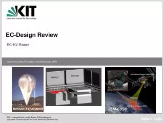
Review of the EC-Front P. Barrillon on behalf of all the people involved (and they are many !) March 1st 2012 - LAL
PDM structure: reminder Dimensions of the PDM frame: 167mm x 167mm x 28.7mm
EC unit description: front part UV filter • 3 different PCBs: • First one (EC DYNODE board) allows to reroute half of the dynodes of 1 MAPMT so that they are aligned perpendicularly to the others. It covers the 4 MAPMTs. • Second one (EC ANODE board) covers one MAPMT but has dimensions reduced allowing a flex pcb to get out. It is used to collect signal from the anodes and send them to the ASICs. • Third one (EC HV board) covers one MAPMT. It welcomes the dynodes and supplies the HV to the EC-dynode board which transmits it to the 4 MAPMTs. MAPMT MAPMT MAPMT • Per EC unit: • 1 EC-DYNODE board • 4 EC-ANODE boards • 1 EC-HV boards Flexible pcb toward EC-back HV cables toward HV box
EC-Unit: side view MAPMT MAPMT dynode EC DYNODE BOARD EC ANODE BOARD anode EC HV BOARD EC-ASIC board welcomes ASICs as well as connectors. Data out are then transmitted to the PDM board. Toward PDM board
From EC-front to EC-back PDM mechanical structure, with cross and hole. The flex and second rigid parts of the EC-anode boards have to go through the mechanical structure to reach the EC-ASIC board.
Dimensions from schematic (Frascati) 6.1 mm outer diameter 3.1 mm inner diameter Radius of the corner : R2.2 17 mm 19.62 mm 19.62 mm 11 mm 6 mm Outer and inner diameters 10 and 6 mm Thickness: 1 mm 55 mm ~2 mm 53 mm 17 mm Thickness: 3 mm 51 mm 9.3 mm Front view
Conclusions from schematic • EC-dynode needs to be < 55 mm long/large 54.5 mm • EC-dynode central hole needs to welcome a screw of 2.5-3 mm • EC-anode flex and 2nd rigid parts needs to be < 19 mm large 16 mm • EC-anode flex needs to be 4-5 cm long depending on the type • The central hole of the mechanical structure can be removed
The EC-dynode board • PCB used to transmit HV signals to the dynodes pins of each MAPMT. • Rerouting will have to be done (inside the pcb) for 7 pins (GR and Dy7 to Dy12) of MAPMT 3 • For the MAPMTs with no rerouting (1, 2 and 4): all 14 pins (K, GR and Dy1 to Dy12) will be cut and soldered on this pcb • For the MAPMT with rerouting (3): the 6 dynodes with lowest voltages and GR will be rerouted, new pins will be soldered on the. These 7 pins and the 7 other ones (Dy1 to Dy6 and K pin) will have extensions added 2 1 3 4 Pins with extensions 64 anodes pins going through the pcb (no soldering/connection) Rerouting of 6 HV pins and GR
EC-dynode: dimensions and pins positions Top view • 54.5 x 54. mm • 1.5 mm thickness (can be reduced to 1.2 mm) • 8 layers pcb • 3.2 mm hole in the middle • 3 areas 16.5 x 2.5 mm added to ease potting spread • bottom right MAPMT print corresponds to the one with the pins extended
EC-dynode: routing Top layer Layer 2 Layer 3 Layer 4 Layer 5 Layer 6 Layer 7 Bottom layer
The EC-anode board (1/3) Bigger holes because of extensions EC-ANODE corresponding to the MAPMT with rerouted pins at the level of the EC-dynode board. Same PCBs (holes for dynodes are not represented) Areas gained for flexes Extensions
The EC-anode board (2/3) Rigid pcb Rigid pcb • Allows the routing of the 64 signals toward the connector. • Choice of the connector is the critical part. It shouldn’t be too high, too large or too long but has to allow a feasible routing. Flexible pcb 23.7 mm connector < 19 cm As long as needed As long as needed ~ 24 mm
The EC-anode board (3/3) C O N N E C TO R C O N N E C TO R • 2 types of pcbs are foreseen: • 1 with a straight flexible part • 1 with a curved flexible part • similar routing • same orientation • One with a connector on top layer, the other with the connector on bottom layer • Easier assembly connector connector
EC-anode: dimensions and pins positions • First rigid: 24 x 23.7 x 1.5 mm • Flex: 16 x 50 x ? mm • Second rigid: 16 x 55 x 1.5 mm • Rigid parts thickness can be reduced to 1.2 mm • Rigid parts: 6 layers pcb • Flex: 4 layers pcb • Holes for the 14 extensions coming from the EC-dynode: 2 mm large.
EC-anode straight: routing Top layer (gnd) Layer 2 Layer 3
EC-anode straight : routing Layer 4 Layer 5 Bottom layer (gnd)
EC-anode curved : routing Layer 3 Layer 2 Top layer (gnd)
EC-anode curved : routing Layer 5 Bottom layer (gnd) Layer 4
EC-HV See Andreas Ebersoldt’s review
EC-front on the mechanical structure MAPMT MAPMT Screws Column • 2 options to fixe the EC front to the PDM mechanical structure: • 2 screws and a column (colonnette in French) in between • 1 screw long enough (~ 20 mm) • In both options the initial central column would be removed. This would ease the assembly and potting of the EC front by postponing the fixation of it on the mechanical structure after the potting. But this central column is part of the initial design which stiffness was proved… • Screws would have 2.5 or 3 mm diameter.
EC front assembly NB: PCBs thickness could be reduced to 1.2 mm 1mm EC-dynode (1.5 mm) 2.5 mm 6.5 mm 11 mm EC-anode (1.5 mm) MAPMT 8.5 mm ~ 3 mm EC-HV (1.5 mm) Soldering (0.5 mm) (7) Added pins, black plastic is 2.5 mm high MAPMT Extensions of the pins
EC front assembly sequence Added pins are soldered to the EC-dynode MAPMT dynodes cut and soldered to the EC-dynode Extensions added to the 14 HV pins coming out of the EC-dynode Anode pins cut (if needed) and soldered to the EC-anode Extensions pins cut and soldered to the EC-HV MAPMT EC-dynode (1.5 mm) EC-anode (1.5 mm) EC-HV (1.5 mm) Soldering (0.5 mm)
The MAPMT (reminder) • R11265-M64 MAPMT from Hamamatsu. • 64 channels (Anodes) • 12 Dynodes (Dy1 – Dy12), 1 cathode (K) and 1 Guard Ring (GR) • It is a photo-detector used to sense the UV photons arriving through the lenses. Each one should be equipped with a UV filter bonded with an optical glue
Potting area Cables going out of the potting Potting must surround the 3 pcbs of the EC-front and the MAPMTs but shouldn’t cover the front of the filters. Potting area Front part of the filters. They must not be covered with potting. MAPMT MAPMT