Download

1 / 63
670 likes | 963 Views
Lecture 3: CMOS Transistor Theory. Outline. Introduction MOS Capacitor nMOS I-V Characteristics pMOS I-V Characteristics Gate and Diffusion Capacitance. Goal of this section. Present intuitive understanding of device operation Introduction of basic device equations

E N D
Outline • Introduction • MOS Capacitor • nMOS I-V Characteristics • pMOS I-V Characteristics • Gate and Diffusion Capacitance 3: CMOS Transistor Theory
Goal of this section • Present intuitive understanding of device operation • Introduction of basic device equations • Introduction of models for manual analysis • Introduction of models for SPICE simulation • Future trends
Diodes • Diodes do not appear in CMOS digital design as separate devices. • However, they are present as junctions and parasitic elements in all devices. • We will use a simple 1D analysis. • We will not concern ourselves too much with the DC behavior too much. 3: CMOS Transistor Theory
DC Characteristics 3: CMOS Transistor Theory
Forward Bias Typically avoided in Digital ICs
Reverse Bias The Dominant Operation Mode
Junction Capacitance 3: CMOS Transistor Theory
Junction Capacitance • m is known as the grading coefficient. • Keep in mind that Cj is a small signal parameter. For large signal switching, an equivalent capacitance has to be calculated as • Ceq has been defined such that the same amount of charge is transferred as the nonlinear model 3: CMOS Transistor Theory
Junction Capacitance • As a numerical example, a diode is switched between 0 and -2.5 V. The diode has Cj0 = 2 X 10⁻³F/m2, AD = 0.5 (mm)2, F0 = 0.64 V, m = 0.5. • Keq = 0.622, Ceq = 1.24 fF/(mm)2. 3: CMOS Transistor Theory
Diffusion Capacitance • Effective in forward bias 3: CMOS Transistor Theory
Diffusion Capacitance • From this lifetime analysis of excess charge, • Note that Cd is also a small signal capacitance 3: CMOS Transistor Theory
Other Diode Parameters • Secondary Effects • Resistivity of regions outside junction • Breakdown voltage • Temperature dependence • FT has a linear dependence • IS doubles every 8˚C • Overall, current doubles every 12˚C. 3: CMOS Transistor Theory
SPICE Model • The following summarize diode behavior: • n is called the emission coefficient and concentrates the non-idealities listed above. 3: CMOS Transistor Theory
Introduction • So far, we have treated transistors as ideal switches • An ON transistor passes a finite amount of current • Depends on terminal voltages • Derive current-voltage (I-V) relationships • Transistor gate, source, drain all have capacitance • I = C (DV/Dt) -> Dt = (C/I) DV • Capacitance and current determine speed 3: CMOS Transistor Theory
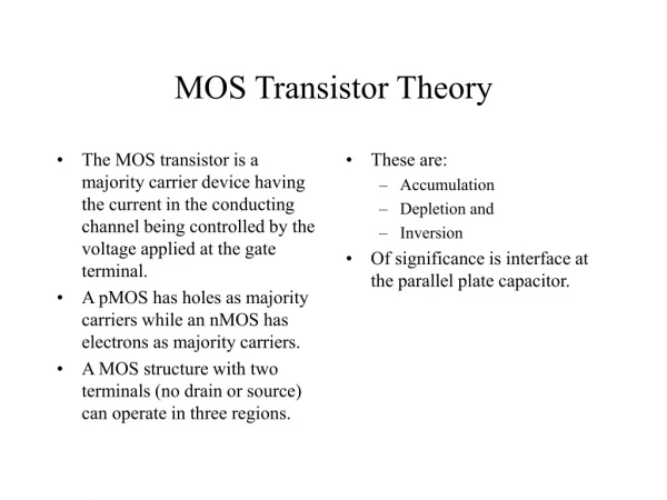
MOS Capacitor • Gate and body form MOS capacitor • Operating modes • Accumulation • Depletion • Inversion 3: CMOS Transistor Theory
Terminal Voltages • Mode of operation depends on Vg, Vd, Vs • Vgs = Vg – Vs • Vgd = Vg – Vd • Vds = Vd – Vs = Vgs - Vgd • Source and drain are symmetric diffusion terminals • By convention, source is terminal at lower voltage • Hence Vds 0 • nMOS body is grounded. First assume source voltage is 0 too. • Three regions of operation • Cutoff • Linear (Resistive) • Saturation (Active) 3: CMOS Transistor Theory
nMOS Cutoff • No channel • Ids≈ 0 3: CMOS Transistor Theory
nMOS Linear • Channel forms • Current flows from d to s • e- from s to d • Ids increases with Vds • Similar to linear resistor 3: CMOS Transistor Theory
nMOS Saturation • Channel pinches off • Ids independent of Vds • We say current saturates • Similar to current source 3: CMOS Transistor Theory
I-V Characteristics • In Linear region, Ids depends on • How much charge is in the channel? • How fast is the charge moving? 3: CMOS Transistor Theory
Channel Charge • MOS structure looks like parallel plate capacitor while operating in inversions • Gate – oxide – channel • Qchannel = CV • C = Cg = eoxWL/tox = CoxWL • V = Vgc – Vt = (Vgs – Vds/2) – Vt Cox = eox / tox 3: CMOS Transistor Theory
Carrier velocity • Charge is carried by e- • Electrons are propelled by the lateral electric field between source and drain • E = Vds/L • Carrier velocity v proportional to lateral E-field • v = mE m called mobility • Time for carrier to cross channel: • t = L / v 3: CMOS Transistor Theory
nMOS Linear I-V • Now we know • How much charge Qchannel is in the channel • How much time t each carrier takes to cross 3: CMOS Transistor Theory
nMOS Saturation I-V • If Vgd < Vt, channel pinches off near drain • When Vds > Vdsat = Vgs – Vt • Now drain voltage no longer increases current 3: CMOS Transistor Theory
nMOS I-V Summary • Shockley 1st order transistor models 3: CMOS Transistor Theory
Example • Your book will be using a 0.6 mm process • From AMI Semiconductor • tox = 100 Å • m = 350 cm2/V*s • Vt = 0.7 V • Plot Ids vs. Vds • Vgs = 0, 1, 2, 3, 4, 5 • Use W/L = 4/2 l 3: CMOS Transistor Theory
pMOS I-V • All dopings and voltages are inverted for pMOS • Source is the more positive terminal • Mobility mp is determined by holes • Typically 2-3x lower than that of electrons mn • 120 cm2/V•s in AMI 0.6 mm process • Thus pMOS must be wider to provide same current • In this class, assume mn / mp = 2 3: CMOS Transistor Theory
Capacitance • Any two conductors separated by an insulator have capacitance • Gate to channel capacitor is very important • Creates channel charge necessary for operation • Source and drain have capacitance to body • Across reverse-biased diodes • Called diffusion capacitance because it is associated with source/drain diffusion 3: CMOS Transistor Theory
Level 1 Implementation in SPICE • Including the channel length modulation, body effect and overlaps, 3: CMOS Transistor Theory
SPICE Model 3: CMOS Transistor Theory
SPICE Model • Electrical parameters override when provided. • Otherwise, they are calculated from physical parameters. • LAMBDA is an empirical parameter. 3: CMOS Transistor Theory
Level 2 Implementation in SPICE • Now, let us remove some of the wrong assumptions. • Voltage across channel is not constant any more • The threshold voltage is not a constant any more 3: CMOS Transistor Theory
Level 2 Implementation in SPICE • To find the equation in the active region, take the derivative of ID and equate to 0. • VDS = VDS,sat when ID is maximum. • Note that ID is dependent on g even if VSB = 0. • VT is not explicitly used in the equations. 3: CMOS Transistor Theory
More Corrections • Mobility is reduced with increasing gate voltage. • We will study this effect in detail later. • Current conduction occurs below the threshold voltage. • We will study this effect later. • Channel length modulation has to be corrected. • Threshold voltage depends on W and L. • Parasitic resistances in the source and drain • Latchup • Speed limit of carriers 3: CMOS Transistor Theory
Speed Limit of Carriers • Ohm’s Law is not true 3: CMOS Transistor Theory
Speed Limit of Carriers • Velocity is proportional to electric field for low fields • Velocity is saturated for high fields • To ensure continuity, use the following approximation for velocity. • Then, 3: CMOS Transistor Theory
Speed Limit of Carriers • That equation is still too complex for hand analysis. • Substitute the values at the critical electric field to find the current at the transition point. • An even simpler approach is as follows 3: CMOS Transistor Theory
Drain-Source Resistance • Large signal drain-source resistance is a nonlinear quantity varying across operating regions. • One can define an equivalent resistance • For a weakly nonlinear function, 3: CMOS Transistor Theory
Drain-Source Resistance • Applying the general formula for a transistor switching from VDD to VDD/2, • Alternatively, using the endpoints and averaging, 3: CMOS Transistor Theory