Download
1 / 11
110 likes | 265 Views
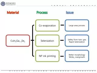
Material. Process. Issue. Co-evaporation. Large area process. CuIn x Ga 1-x Se 2. Selenization. Safety from toxic gas Rapid Selenization. NP ink printing. Better morphology MoSe 2 overgrowth. Material. CuIn x Ga 1-x Se 2. Process. Microstructure. Performance. NP printing /

E N D
Material Process Issue Co-evaporation Large area process CuInxGa1-xSe2 Selenization Safety from toxic gas Rapid Selenization NP ink printing Better morphology MoSe2 overgrowth
Material CuInxGa1-xSe2 Process Microstructure Performance NP printing / Sintering Porous morphology Thick MoSe2 Low JSC Poor FF Analysis Analysis Phase transformation that includes Melting & Evaporation Sintering mechanism Driving force Mass transport MoSe2 growth Direct reaction between Mo and Se (Pore) Surface trap Trap-enhanced recombination Series resistance Thickness and crystal orientation of MoSe2 Feedback
Idea for morphology improvement • Instant melting of CIGS particulate precursor by thermal plasma Ex) CIS film formed by spot welding of Cu,In,Se particles (Thin Solid Films, 517, 2184)
Material CuInxGa1-xSe2 Process Microstructure Performance Metal deposition / Selenization Multiphase film / Ga segregation Eff. ~ 14% Analysis Analysis Diffusion Modeling In-situ investigation Insufficient bandgap optimization Feedback
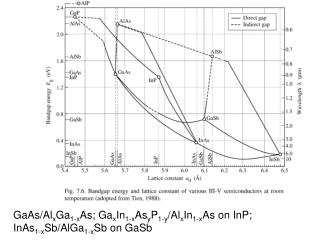
Selenization Phases, morphology, and diffusion in CuInxGa1-xSe2 thin films JAP, 82, 2896 (1997) Precursor film Phase & morphology Diffusion CuInSe2 CuGaSe2 Phase and morphology analysis Annealed film CuInxGa1-xSe2 Selenized film
Two-step process To introduce selenium… For large scale process… Metal sputtering Selenization To improve morphology… For low cost process… Nanoparticle printing Sintering To form compound… For Se-free process… Multi-layer Selenide deposition Homogenization
If we have efficient large-area deposition process for selenide compound… Why we have to use two-step process Instead of one-step co-deposition?
FASSTTM process Merits of process : Flexibility (Separate optimization of each layers) Prevent selenium loss (by given mechanical pressure) At present… HelioVolt is developing nanoparticle printing process
Compared to CuInSe2, selenide precursorscan have much lower melting point → Much easier sintering at low temperature