CT455: Computer Organization Logic gate
CT455: Computer Organization Logic gate. Lecture 4: Logic Gates and Circuits. Logic Gates The Inverter The AND Gate The OR Gate The NAND Gate The NOR Gate The XOR Gate The XNOR Gate Drawing Logic Circuit Analysing Logic Circuit Propagation Delay. Lecture 4: Logic Gates and Circuits.

CT455: Computer Organization Logic gate
E N D
Presentation Transcript
Lecture 4:Logic Gates and Circuits • Logic Gates • The Inverter • The AND Gate • The OR Gate • The NAND Gate • The NOR Gate • The XOR Gate • The XNOR Gate • Drawing Logic Circuit • Analysing Logic Circuit • Propagation Delay
Lecture 4: Logic Gates and Circuits • Universal Gates: NAND and NOR • NAND Gate • NOR Gate • Implementation using NAND Gates • Implementation using NOR Gates • Implementation of SOP Expressions • Implementation of POS Expressions • Positive and Negative Logic • Integrated Circuit Logic Families
Digital (logic) Elements: Gates • Digital devices or gates have one or more inputs and produce an output that is a function of the current input value(s). • All inputs and outputs are binary and can only take the values 0 or 1 • A gate is called a combinational circuit because the output only depends on the current input combination. • Digital circuits are created by using a number of connected gates such as the output of a gate is connected to to the input of one or more gates in such a way to achieve specific outputs for input values. • Digital or logic design is concerned with the design of such circuits.
Introduction • Hardware consists of a few simple building blocks • These are called logic gates • AND, OR, NOT, … • NAND, NOR, XOR, … • Logic gates are built using transistors • NOT gate can be implemented by a single transistor • AND gate requires 3 transistors • Transistors are the fundamental devices • Pentium consists of 3 million transistors • Compaq Alpha consists of 9 million transistors • Now we can build chips with more than 100 million transistors Chapter 1: Introduction
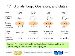
Symbol set 2 (ANSI/IEEE Standard 91-1984) Symbol set 1 a b AND & a.b a b a.b OR a b 1 a+b a b a+b NOT a a' 1 a a' a b a b (a.b)' & NAND (a.b)' a b a b NOR (a+b)' 1 (a+b)' a b a b =1 a b a b Logic Gates • Gate Symbols EXCLUSIVE OR
x y x . y x + y 0 0 0 0 0 1 0 1 1 0 0 1 1 1 1 1 Truth Tables • Provides a listing of every possible combination of values of binary inputs to a digital circuit and the corresponding outputs. • Example (2 inputs, 2 outputs): Truth table inputs outputs inputs outputs x x . y Digital circuit y x + y
Basic Concepts • Simple gates • AND • OR • NOT • Functionality can be expressed by a truth table • A truth table lists output for each possible input combination • Other methods • Logic expressions • Logic diagrams Chapter 1: Introduction
Basic Concepts (cont’d) • Additional useful gates • NAND • NOR • XOR • NAND = AND + NOT • NOR = OR + NOT • XOR implements exclusive-OR function • NAND and NOR gates require only 2 transistors • AND and OR need 3 transistors! Chapter 1: Introduction
Realizing Logic in Hardware • Boolean Algebra and truth tables are essential important tools to express logical relationships. • To use these tools in the real world , we must have some physical way to represent TRUE and FALSE (T and F). • In, digital electronic circuits, T and F are represented by voltage levels: • The transistor-transistor logic (TTL) 74LS family of digital integrated circuits produces two voltage levels: • < .5V which represents low voltage L (0) and, • > 2.7V which represents high voltage H (1) for the digital device.
Electronic Logic Gates • Electrical Signals and Logic Values • A signal that is set to logic 1 is said to be asserted, active, or true. • An active-high signal is asserted when it is high (positive logic). • An active-low signal is asserted when it is low (negative logic). Chapter 1: Introduction
A A' A A' Binary number 0 0 1 1 0 1 1 0 1 1 0 1 0 0 1 0 1’s Complement Logic Gates: The Inverter • The Inverter • Application of the inverter: complement.
A B A B & A.B A.B Logic Gates: The AND Gate • The AND Gate
1 sec A A Counter Enable Enable 1 sec Register, decode and frequency display Reset to zero between Enable pulses Logic Gates: The AND Gate • Application of the AND Gate
A B A B 1 A+B A+B Logic Gates: The OR Gate • The OR Gate
A B A B A B (A.B)' (A.B)' (A.B)' & NAND Negative-OR Logic Gates: The NAND Gate • The NAND Gate
A B A B A B (A+B)' (A+B)' (A+B)' 1 NOR Negative-AND Logic Gates: The NOR Gate • The NOR Gate
A B A B =1 A B A B Logic Gates: The XOR Gate • The XOR Gate
A B A B =1 (A B)' (A B)' Logic Gates: The XNOR Gate • The XNOR Gate
Basic Concepts (cont’d) • Proving NAND gate is universal Chapter 1: Introduction
Basic Concepts (cont’d) • Proving NOR gate is universal Chapter 1: Introduction
x y F1 z' z Drawing Logic Circuit • When a Boolean expression is provided, we can easily draw the logic circuit. • Examples: (i) F1 = xyz' (note the use of a 3-input AND gate)
x F2 y' z y'z x xy' y' F3 x' z x'z Drawing Logic Circuit (ii) F2 = x + y'z (can assume that variables and their complements are available) (iii) F3 = xy' + x'z
A' B' C F4 Analysing Logic Circuit • When a logic circuit is provided, we can analyse the circuit to obtain the logic expression. • Example: What is the Boolean expression of F4? A'B' A'B'+C (A'B'+C)' F4 = (A'B'+C)' = (A+B).C'
Logic Functions (cont’d) 3-input majority function A B C F 0 0 0 0 0 0 1 0 0 1 0 0 0 1 1 1 1 0 0 0 1 0 1 1 1 1 0 1 1 1 1 1 • Logical expression form F = A B + B C + A C Chapter 1: Introduction
Propagation Delay • Every logic gate experiences some delay (though very small) in propagating signals forward. • This delay is called Gate (Propagation) Delay. • Formally, it is the average transition time taken for the output signal of the gate to change in response to changes in the input signals. • Three different propagation delay times associated with a logic gate: • tPHL: output changing from the High level to Low level • tPLH: output changing from the Low level to High level • tPD=(tPLH + tPHL)/2 (average propagation delay)
Input Output H Input L H Output L tPHL tPLH Propagation Delay
A B C • In reality, output signals normally lag behind input signals: 1 1 Signal for A Signal for A 0 0 1 1 Signal for B Signal for B 0 0 1 1 Signal for C Signal for C 0 0 time time Propagation Delay • Ideally, no delay:
Calculation of Circuit Delays • Amount of propagation delay per gate depends on: • (i) gate type (AND, OR, NOT, etc) • (ii) transistor technology used (TTL,ECL,CMOS etc), • (iii) miniaturisation (SSI, MSI, LSI, VLSI) • To simplify matters, one can assume • (i) an average delay time per gate, or • (ii) an average delay time per gate-type. • Propagation delay of logic circuit = longest time it takes for the input signal(s) to propagate to the output(s). = earliest time for output signal(s) to stabilise, given that input signals are stable at time 0.
t1 t2 Logic Gate : : tn max (t1, t2, ..., tn ) + t Calculation of Circuit Delays • In general, given a logic gate with delay, t. If inputs are stable at times t1,t2,..,tn, respectively; then the earliest time in which the output will be stable is: max(t1, t2, .., tn) + t • To calculate the delays of all outputs of a combinational circuit, repeat above rule for all gates.
0 max(0,0)+t = t X Y max(t,0)+t = 2t 0 S t 2t max(t,2t)+t = 3t C 0 Z Calculation of Circuit Delays • As a simple example, consider the full adder circuit where all inputs are available at time 0. (Assume each gate has delay t.) where outputs S and C, experience delays of 2t and 3t, respectively.
Universal Gates: NAND and NOR • AND/OR/NOT gates are sufficient for building any Boolean functions. • We call the set {AND, OR, NOT} a complete set of logic. • However, other gates are also used because: (i) usefulness (ii) economical on transistors (iii) self-sufficient NAND/NOR: economical, self-sufficient XOR: useful (e.g. parity bit generation)
x x' NAND Gate • NAND gate is self-sufficient (can build any logic circuit with it). • Therefore, {NAND} is also a complete set of logic. • Can be used to implement AND/OR/NOT. • Implementing an inverter using NAND gate: (x.x)' = x' (T1: idempotency)
(x.y)' x x.y y x' x x+y y y' NAND Gate • Implementing AND using NAND gates: ((xy)'(xy)')' = ((xy)')' idempotency = (xy) involution • Implementing OR using NAND gates: ((xx)'(yy)')' = (x'y')' idempotency = x''+y'' DeMorgan = x+y involution
x x' NOR Gate • NOR gate is also self-sufficient. • Therefore, {NOR} is also a complete set of logic • Can be used to implement AND/OR/NOT. • Implementing an inverter using NOR gate: (x+x)' = x' (T1: idempotency)
(x+y)' x' x x x+y y x.y y y' NOR Gate • Implementing AND using NOR gates: ((x+x)'+(y+y)')'=(x'+y')' idempotency = x''.y'' DeMorgan = x.y involution • Implementing OR using NOR gates: ((x+y)'+(x+y)')' = ((x+y)')' idempotency = (x+y) involution
Implementation using NAND gates • Possible to implement any Boolean expression using NAND gates. Procedure: (i) Obtain sum-of-products Boolean expression: e.g. F3 = xy'+x'z (ii) Use DeMorgan theorem to obtain expression using 2-level NAND gates e.g. F3 = xy'+x'z = (xy'+x'z)' ' involution = ((xy')' . (x'z)')' DeMorgan
x (xy')' y' F3 x' (x'z)' z Implementation using NAND gates F3 = ((xy')'.(x'z)') ' = xy' + x'z
Implementation using NOR gates • Possible to implement any Boolean expression using NOR gates. Procedure: (i) Obtain product-of-sums Boolean expression: e.g. F6 = (x+y').(x'+z) (ii) Use DeMorgan theorem to obtain expression using 2-level NOR gates. e.g. F6 = (x+y').(x'+z) = ((x+y').(x'+z))' ' involution = ((x+y')'+(x'+z)')' DeMorgan
x (x+y')' y' F6 x' (x'+z)' z Implementation using NOR gates F6 = ((x+y')'+(x'+z)')' = (x+y').(x'+z)
Logical Equivalence • All three circuits implement F = A B function Chapter 1: Introduction
Logical Equivalence (cont’d) • Derivation of logical expression from a circuit • Trace from the input to output • Write down intermediate logical expressions along the path Chapter 1: Introduction
Logical Equivalence (cont’d) • Proving logical equivalence: Truth table method A B F1 = A B F3 = (A + B) (A + B) (A + B) 0 0 0 0 0 1 0 0 1 0 0 0 1 1 1 1 Chapter 1: Introduction
A B C F D E Implementation of SOP Expressions • Sum-of-Products expressions can be implemented using: • 2-level AND-OR logic circuits • 2-level NAND logic circuits • AND-OR logic circuit F = AB + CD + E
A B C F D E A B C F D E' Implementation of SOP Expressions • NAND-NAND circuit (by circuit transformation) a) add double bubbles b) change OR-with- inverted-inputs to NAND & bubbles at inputs to their complements
Deriving Logical Expressions (cont’d) • 3-input majority function A B C F 0 0 0 0 0 0 1 0 0 1 0 0 0 1 1 1 1 0 0 0 1 0 1 1 1 1 0 1 1 1 1 1 • SOP logical expression • Four product terms • Because there are 4 rows with a 1 output F = A B C + A B C +A B C + A B C • Sigma notation S(3, 5, 6, 7) Chapter 1: Introduction
Brute Force Method of Implementation 3-input even-parity function A B C F 0 0 0 0 0 0 1 1 0 1 0 1 0 1 1 0 1 0 0 1 1 0 1 0 1 1 0 0 1 1 1 1 • SOP implementation Chapter 1: Introduction
A B C G D E Implementation of POS Expressions • Product-of-Sums expressions can be implemented using: • 2-level OR-AND logic circuits • 2-level NOR logic circuits • OR-AND logic circuit G = (A+B).(C+D).E
A B C G D E A B C G D E' Implementation of POS Expressions • NOR-NOR circuit (by circuit transformation): a) add double bubbles b) changed AND-with- inverted-inputs to NOR & bubbles at inputs to their complements
Deriving Logical Expressions (cont’d) • 3-input majority function A B C F 0 0 0 0 0 0 1 0 0 1 0 0 0 1 1 1 1 0 0 0 1 0 1 1 1 1 0 1 1 1 1 1 • POS logical expression • Four sum terms • Because there are 4 rows with a 0 output F = (A + B + C) (A + B + C) (A + B + C) (A + B + C) • Pi notation (0, 1, 2, 4 ) Chapter 1: Introduction