EE 261 – Introduction to Logic Circuits
360 likes | 577 Views
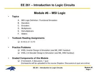
EE 261 – Introduction to Logic Circuits. Module #6 – MSI Logic Topics MSI Logic Definition / Functional Simulation Decoders Encoders Multiplexers Demultiplexers Adders Textbook Reading Assignments 6.4-6.5, 6.7, 6.10 Practice Problems

EE 261 – Introduction to Logic Circuits
E N D
Presentation Transcript
EE 261 – Introduction to Logic Circuits Module #6 – MSI Logic • Topics • MSI Logic Definition / Functional Simulation • Decoders • Encoders • Multiplexers • Demultiplexers • Adders • Textbook Reading Assignments • 6.4-6.5, 6.7, 6.10 • Practice Problems • VHDL Inverter Design & Simulation (see M6_HW1 handout) • VHDL 2:4 Decoder Design & Simulation (see M6_HW2 handout) • Graded Components of this Module • 2 homework, 2 discussion, 1 quiz(homeworks will be uploaded to the course Dropbox. Discussions & quiz are online)
EE 261 – Introduction to Logic Circuits Module #6 – MSI Logic • What you should be able to do after this module • Understand the operation of Decoders, Encoders, Multiplexers, Demultiplexers,and Adders • Synthesizes the gate level schematic for each of these MSI circuits • Use VHDL to describe and simulate the MSI circuits covered in this module
Integrated Circuit Scaling • Integrated Circuit ScalesExample# of TransistorsSSI - Small Scale Integrated Circuits Individual Gates 10's MSI - Medium Scale Integrated Circuits Mux, Decoder 100'sLSI - Large Scale Integrated Circuits RAM, ALU's 1k - 10kVLSI - Very Large Scale Integrated Circuits uP, uCNT 100k - 1M- we use the terms SSI and MSI. Everything larger is typically just called "VLSI"- VLSI covers design that can't be done using schematics or by hand.
Decoders • Decoders- a decoder has n inputs and 2n outputs- one and only one output is asserted for a given input combinationex) truth table of decoder “Inputs” “Outputs”A BY3 Y2 Y1 Y0 0 0 0 0 0 1 0 1 0 0 1 0 1 0 0 1 0 0 1 1 1 0 0 0- To design the gate level circuitry, we write a logic expression for EACH INDIVIDUAL OUTPUT- Remember that Boolean Algebra & K-maps produce a 1-bit output expression.
Decoder • Decoder Structure- The output stage of a decoder can be constructed using AND gates- Inverters are needed to give the appropriate code to each AND gate- Using AND/INV structure, we need: 2n AND gates n InvertersA BY3 Y2 Y1 Y0 0 0 0 0 0 1 0 1 0 0 1 0 1 0 0 1 0 0 1 1 1 0 0 0 A B 0 1 1 0 0 2 0 Y0 = A’·B’ 0 1 3 0 1 A B 0 1 0 0 0 2 0 Y1 = A’·B 1 1 0 3 1 A B 0 1 0 0 1 2 0 Y2 = A·B’ 0 1 0 3 1 A B 0 1 0 0 0 2 0 Y3 = A·B 1 0 1 3 1 Showing more inverters than necessary to illustrate concept
Decoders in Structural VHDL • Decoder Example - Let's design a 2-to-4 Decoder using Structural VHDL (i.e., connecting AND and INV components)- We know we need to describe the following structure:- We know what we'll need: 2n AND gates = 4 AND gates n Inverters = 2 Inverters Showing more inverters than necessary to illustrate concept
Decoders in Structural VHDL • Decoder Example- Let's design the inverter using concurrent signal assignments….entity inv is port (In1 : in BIT; Out1 : out BIT); end entity inv;architecture inv_arch of inv is begin Out1 <= not In1; end architecture inv_arch;
Decoders in Structural VHDL • Decoder Example- Let's design the AND gate using concurrent signal assignments….entity and2 is port (In1,In2 : in BIT; Out1 : out BIT); end entity and2;architecture and2_arch of and2 is begin Out1 <= In1 and In2; end architecture and2_arch;
Decoders in Structural VHDL • Decoder Example- Now let's work on the top level design entity called "decoder_2to4"entity decoder_2to4 is port (A,B : in BIT; Y0,Y1,Y2,Y3 : out BIT); end entity decoder_2to4;
Decoders in Structural VHDL • Decoder Example- Now let's work on the top level design architecture called "decoder_2to4_arch"architecture decoder_2to4 _arch of decoder_2to4 is signal A_n, B_n : BIT; component inv port (In1 : in BIT; Out1 : out BIT); end component; component and2 port (In1,In2 : in BIT; Out1 : out BIT); end component; begin ………
Decoders in Structural VHDL • Decoder Example- cont…. begin U1 : inv port map (A, A_n); U2 : inv port map (B, B_n); U3 : and2 port map (A_n, B_n, Y0); U4 : and2 port map (A, B_n, Y1); U5 : and2 port map (A_n, B, Y2); U6 : and2 port map (A, B, Y3);end architecture decoder_2to4 _arch;
Decoders in Behavioral VHDL • Decoder Example - Let's design a 2-to-4 Decoder using Behavioral VHDL (i.e., using signal assignments & operators) - Now let's work on the top level design architecture called "decoder_2to4_arch"entity decoder_2to4 is port (A,B : in BIT; Y0,Y1,Y2,Y3 : out BIT); end entity decoder_2to4;architecture decoder_2to4 _arch of decoder_2to4 is begin Y0 <= (not A) and (not B); Y1 <= (not A) and (B); Y2 <= (A) and (not B); Y3 <= (A) and (B);end architecture decoder_2to4 _arch;
Decoders in VHDL • Decoder Example - What would this look like in a functional simulation? 1 and only 1 output is asserted for each 2-bit input code
Encoders • Encoder- an encoder has 2n inputs and n outputs- it assumes that one and only one input will be asserted- depending on which input is asserted, an output code will be generated- this is the exact opposite of a decoder ex) truth table of binary encoderInput Output 0001 00 0010 01 0100 10 1000 11
Encoders • Encoder- an encoder output is a simple OR structure that looks at the incoming signals ex) 4-to-2 encoderI3 I2 I1 I0Y1 Y0 0 0 0 1 0 0 0 0 1 0 0 1 0 1 0 0 1 0 1 0 0 0 1 1 Y1 = I3 + I2 Y0 = I3 + I1 I3 I2 I1 I0 00 01 11 10 0 x 1 4 x 12 8 1 00 1 0 5 x 13 x 9 x 01 Y1 = I3 +I2 x 3 x 7 15 x x 11 11 2 0 x 6 x 14 x 10 10 I3 I2 I1 I0 00 01 11 10 x 0 4 0 12 x 1 8 00 1 0 5 x x 13 9 x 01 Y0 = I3 +I1 3 x 7 x 15 x x 11 11 2 1 6 x x 14 10 x 10
Encoders in Structural VHDL • Encoders in VHDL- 8-to-3 binary encoder modeled with Structural VHDL entity encoder_8to3_binary is port (I : in BIT_VECTOR (7 downto 0); Y : out BIT_VECTOR (2 downto 0) ); end entity encoder_8to3_binary; architecture encoder_8to3_binary_arch of encoder_8to3_binary is component or4 port (In1,In2,In3,In4: in BIT; Out1: out BIT); end component; begin U1 : or4 port map (In1 => I(1), In2 => I(3), In3 => I(5), In4 => I(7), Out1 => Y(0) ); U2 : or4 port map (In1 => I(2), In2 => I(3), In3 => I(6), In4 => I(7), Out1 => Y(1) ); U3 : or4 port map (In1 => I(4), In2 => I(5), In3 => I(6), In4 => I(7), Out1 => Y(2) ); end architecture encoder_8to3_binary_arch;
Multiplexer • Multiplexer- gates are combinational logic which generate an output depending on the current inputs- what if we wanted to create a “Digital Switch” to pass along the input signal?- this type of circuit is called a “Multiplexer” ex) truth table of Multiplexer SelOut0 A 1 B
Multiplexer • Multiplexer- the outputs will track the selected input- this is in effect, a “Switch”ex) truth table of MultiplexerSelA BOut 0 0 x 0 0 1 x 1 1 x 0 0 1 x 1 1
Multiplexer • Multiplexer- we can use the behavior of an AND gate to build this circuit: X∙0 = 0 “Block Signal”X∙1 = X “Pass Signal”- we can then use the behavior of an OR gate at the output state (since a 0 input has no effect) to combine the signals into one output 0 A 0 1 =B =A B 0 1 0 1 0
Multiplexer • Multiplexer- if we wanted to explicitly form the logic expression, we could use a verbose truth table that lists each possible input value for A and BSelOut 0 A 1 B Sel A BOut0 0 0 00 0 1 0 0 1 0 1 0 1 1 1 1 0 0 0 1 0 1 1 1 1 0 0 1 1 1 1 Sel A B 00 01 11 10 0 0 1 2 6 0 0 4 0 1 0 3 1 1 7 1 5 1 Out = Sel’·A + Sel·B
Multiplexer in Structural VHDL • 2-to-1 Multiplexers in Structural VHDL- Structural Model D(0) U2_out U2 Sel_n Y U4 entity mux_2to1 is port (D : in BIT_VECTOR (1 downto 0); Sel : in BIT; Y : out BIT); end entity mux_2to1; architecture mux_2to1_arch of mux_2to1 is signal Sel_n : BIT; signal U2_out, U3_out : BIT; component inv1 port (In1: BIT; Out1: out BIT); end component; component and2 port (In1,In2 : in BIT; Out1: out BIT); end component; component or2 port (In1,In2 : in BIT; Out1: out BIT); end component; begin U1 : inv1 port map (In1 => Sel, Out1 => Sel_n); U2 : and2 port map (In1 => D(0), In2 => Sel_n, Out1 => U2_out); U3 : and2 port map (In1 => D(1), In2 => Sel, Out1 => U3_out); U4 : or4 port map (In1 => U2_out, In2 => U3_out, Out1 => Y); end architecture mux_2to1_arch; D(1) U3 U3_out U1
Multiplexer in Behavioral VHDL • 2-to-1 Multiplexers in Behavioral VHDL (Conditional Signal Assignments)- Behavioral Model entity mux_2to1 is port (D : in BIT_VECTOR (1 downto 0); Sel : in BIT; Y : out BIT_LOGIC); end entity mux_2to1; architecture mux_2to1_arch of mux_2to1 is begin Y <= D(0) when Sel=‘0’ else D(1); end architecture mux_2to1_arch;
Multiplexer in Behavioral VHDL • 2-to-1 Multiplexers in Behavioral VHDL (Selected Signal Assignments)- Behavioral Model entity mux_2to1 is port (D : in BIT_VECTOR (1 downto 0); Sel : in BIT; Y : out BIT_LOGIC); end entity mux_2to1; architecture mux_2to1_arch of mux_2to1 is begin with Sel select Y <= D(0) when ‘0’, D(1) when ‘1’; end architecture mux_2to1_arch;
Demultiplexer • Demultiplexer- this is the exact opposite of a Mux- a single input will be routed to a particular output pin depending on the Select settingex) truth table of DemultiplexerSelY0 Y1 0 In 0 1 0 In
Demultiplexer • Demultiplexer- we can again use the behavior of an AND gate to “pass” or “block” the input signal- an AND gate is used for each DemuxoutputSel In Y0 Y1 0 0 0 0 0 1 1 0 1 0 0 0 1 1 0 1 Sel In 0 1 0 0 0 2 0 Y0 = Sel’·In 1 1 3 0 1 Sel In 0 1 0 0 0 2 0 Y1 = Sel·In 1 0 1 3 1
Demultiplexer in Structural VHDL • Demultiplexers in VHDL- Structural Model D Sel_n U2 D U3 entity demux_1to2 is port (D : in BIT; Sel: in BIT; Y : out BIT_VECTOR (1 downto 0)); end entity demux_1to2; architecture demux_1to2_arch of demux_1to2 is signal Sel_n: BIT; component inv1 port (In1: in BIT; Out1: out BIT); end component; component and2 port (In1,In2: in BIT; Out1: out BIT); end component; begin U1 : inv1 port map (In1 => Sel, Out1 => Sel_n); U2 : and2 port map (In1 => D, In2 => Sel_n, Out1 => Y(0)); U3 : and2 port map (In1 => D, In2 => Sel, Out1 => Y(1)); end architecture demux_1to2_arch; U1
Demultiplexer in Behavioral VHDL • Demultiplexers in VHDL- Behavioral Model D D entity demux_1to2 is port (D : in BIT; Sel: in BIT; Y : out BIT_VECTOR (1 downto 0)); end entity demux_1to2; architecture demux_1to2_arch of demux_1to2 is begin Y(0) <= D and (not Sel); Y(1) <= D and Sel; end architecture demux_1to2_arch;
MSI Adders • Remembering Binary Addition- Let’s start with 1-bit Addition. 0 1 0 1 +0+0+1+1 0 1 1 10- Notice that one of the additions (1+1) generated a “Carry”.- We want to build a circuit that can add two inputs and create the Sum and Carry (Cout).- Let’s list out the Truth Table for our circuit:A BSum Cout 0 0 0 0 0 1 1 0 By inspection, we see that: 1 0 1 0 1 1 0 1 Sum = A BCout = A· B
MSI Adders • Binary Addition- We call this a “Half Adder” because it doesn’t consider a Carry-In from a prior addition Sum = A BCout = A· B - If we wanted to start doing multi-bit addition (i.e., n-bits + n-bits), we need to handle the Carry-Out from the prior bit position addition.- If we consider the “Carry-In”, we now have a 3-input circuit called a “Full Adder”Cin A BCout Sum 0 0 0 0 0 0 0 1 0 1 0 1 0 0 1 0 1 1 1 0 1 0 0 0 1 1 0 1 1 0 1 1 0 1 0 1 1 1 1 1
MSI Adders • Binary Addition- If we can make a Full Adder, we can chain them together to perform multi-bit addition- This is called a “Ripple Carry Adder”, because each subsequent stage needs to wait until the Cout in generated by the prior state. The Cout from the prior stage is then used as the current stage’s Cin.
MSI Adders • Full Adders- Let’s look at the circuitry for a Full Adder:Cin A BCoutSum 0 0 0 0 0 0 0 1 0 1 0 1 0 0 1 0 1 1 1 0 1 0 0 0 1 1 0 1 1 0 1 1 0 1 0 1 1 1 1 1 Cin A B 00 01 11 10 0 0 2 1 0 6 4 1 0 1 1 3 0 1 7 0 5 1 Sum = Cin’·A’·B + Cin’·A·B’ + Cin·A·B + Cin·A’·B’ Cin A B 00 01 11 10 0 0 2 0 1 6 0 4 0 1 0 3 1 1 7 1 5 1 Cout = Cin·A + A·B + Cin·B
MSI Adders • Full Adders- We can accomplish the Full Adder using these logic expression. But could we do it with Half Adders?- Let’s start by manipulating the expression for “Sum”Sum = Cin’·A’·B + Cin’·A·B’ + Cin·A·B + Cin·A’·B’ Sum = A’·(Cin’·B +Cin·B’) + A·(Cin’·B’ + Cin·B) factor out A and A’ Notice that (Cin’·B’ + Cin·B) = (Cin B)’ i.e., an XNOR Notice that (Cin’·B + Cin·B’) = (Cin B), i.e, an XORSum = A’·(Cin B) + A·(Cin B)’ Notice that this is ALSO an XOR. For example, if X=(Cin B), then we would have: Sum = A’·X + A·X’ = A X Sum = A (Cin B) Rearranging…Sum = (A B) Cin - Since the Sum of a “Half Adder” is A B, we can use two Half Adders to produce the Full Adder Sum
MSI Adders • Full Adder using Two Half Adders- Now we have the Sum taken care of, but what about the Carry Out?
MSI Adders • Full Adders using Two Half Adders- Let’s look at some of the intermediate logic expressions: 1st Half 2nd Half Full Adder Adder Adder OutputCin A BCout SumCout Sum Cout Sum 0 0 0 0 0 0 0 0 0 0 0 1 0 1 0 1 0 1 0 1 0 0 1 0 1 0 1 0 1 1 1 0 0 0 1 0 1 0 0 0 0 0 1 0 1 1 0 1 0 1 1 0 1 0 1 1 0 0 1 1 0 1 0 1 1 1 1 0 0 1 1 1 This is what we originally wanted for Sum, so this proves our Full Adder “Sum” is correct.
MSI Adders • Full Adders using Two Half Adders- Notice the Cout Expression: 1st Half 2nd Half Full Adder Adder Adder OutputCin A BCout SumCout Sum Cout Sum 0 0 0 0 0 0 0 0 0 0 0 1 0 1 0 1 0 1 0 1 0 0 1 0 1 0 1 0 1 1 1 0 0 0 1 0 1 0 0 0 0 0 1 0 1 1 0 1 0 1 1 0 1 0 1 1 0 0 1 1 0 1 0 1 1 1 1 0 0 1 1 1 Cout (Full Adder) = Cout (1st Half Adder) + Cout (2nd Half Adder)
MSI Adders • Full Adders using Two Half Adders- This gives us our final Full Adder Circuit using: 2 Half Adders (2x XOR, 2x AND) 1 OR Gate