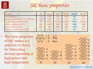
SiC basic properties
SiC basic properties. Property Band gap (eV) Breakdown field for 10 17 cm -3 (MV/cm) Saturated Electron Drift (cm/s) Electron mobility (cm 2 /Vs) Hole mobility (cm 2 /Vs) Thermal Conductivity (W/cmK). Si 1.1 0.6 10 7 1350 450 1.5. GaAs 1.42 0.65 1x10 7 6000 330 0.46. GaN

SiC basic properties
E N D
Presentation Transcript
SiC basic properties Property Band gap (eV) Breakdown field for 1017cm-3 (MV/cm) Saturated Electron Drift (cm/s) Electron mobility (cm2/Vs) Hole mobility (cm2/Vs) Thermal Conductivity (W/cmK) Si 1.1 0.6 107 1350 450 1.5 GaAs 1.42 0.65 1x10⁷ 6000 330 0.46 GaN 3.4 3.5 1.5x10⁷ 1000 300 1.3 3C-SiC 2.36 1.5 2.5x10⁷ <800 <320 5.0 4H-SiC 3.2 3-5 2x10⁷ <900 <120 4.9 6H-SiC 3.0 3-5 2.5x10⁷ <400 <90 4.9 • The basic properties of SiC makes it a material of choice for fabricating devices operating at high power and high temperature
SiC growth processes • DPB defects result from change in stacking of atomic layers in hetero-epitaxial growth Figure modified after Matsunami et al., Amorphous and Crystalline Silicon Carbide, Springer-Verlag, Proceedings in Physics, V. 34 (1989) pp. 34-39.
SiC growth features AFM image of SiC epilayer growth showing step bunching AFM image around a dislocation core in 4H-SiC 0.5 nm (two Si-C bilayers) and 1.0 nm (4 Si-C bilayers = 4H-SiC repeat distance) step features are clearly revealed around screw dislocation core.
SiC devices: Comparison with GaN • Mostly used for high power microwave devices (L, S, C-band amplifiers) • Applications in high power and high temperature electronics (HEV circuits, engine sensors, power schottky and p-n diode rectifiers etc.) • Advantages compared to GaN: • More mature technology than GaN • Bipolar devices (Thyristors, BJTs, DIMOS much more feasible) • Native substrate available, high thermal conductivity • Easier processing than GaN • Disadvantages compared to GaN: • Indirect bandgap material, lower mobility, no HFET • Polytypism, even native substrates have large area defects • Expensive • Growth not easy due to high temperature process
0.26 μm n-type channel layer Doping ~2 1017 cm-3 0.25 μm p-type buffer layer Doping < 5 1015 cm-3 4H-SiC substrate (Vanadium doped) SiC based MESFETs Layer structure • Growth is easier due to lattice matched substrate. Also higher thermal conductivity. • Have higher input and output impedances, so easier to design broadband matching networks • Power output up to 6-7 W/mm • Due to lower mobility of SiC Ft usually not more than 20 GHz. (as 2DEG not possible) • Acceptable noise figure and linearity Small periphery (2300 m)
SiC based power electronics Gate Asymmetrical gate turn off thyristor structure for SiC Anode Gate Gate • 3100 V, 20 A, 62 kW-pulsed, single cell SiC Thyristors demonstrated • Advantage of SiC is much higher power operation due to wider bandgap of SiC P+ N+ N+ N NJTE NJTE P- 2 mm 50 mm, 7-9x1014 cm-3 J3 P+ N+ N+ 4H-SiC Substrate Cathode Anode
SiC based schottky diode gas sensors A SiC schottky diode for H2 gas sensing • Devices made from wide bandgap materials such as SiC and GaN are sensitive to gases such as H2, CO and NO2. • The basic mechanism for such sensing is that the schottky barrier height is lowered as the gas gets absorbed by the schottky barrier. • Very useful for fire detection, and gas sensing in hightemperature environment
Few final things • The final is on 10th December starting at 9.00 a.m. • The presentation to be determined by alphabetical sequence of the Last Name (3 on Wednesday and 3 on Friday) • Each presentation will be 15 minutes • The project report is due by Friday morning, 12th December (I need to submit grades by Friday). • Good Luck!