Download
1 / 7
70 likes | 204 Views
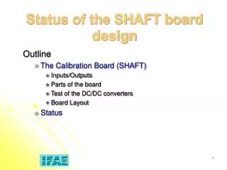
Status of the SHAFT board design. Outline The Calibration Board (SHAFT) Inputs/Outputs Parts of the board Test of the DC/DC converters Board Layout Status. INPUTS_OUTPUTS. Total Inputs: 7 NIM, 1 LVDS, 1 ECL. Total Outputs: 8 NIM, 4 LVDS, 2 ECL. PARTS OF THE BOARD.

E N D
Status of the SHAFT board design Outline The Calibration Board (SHAFT) Inputs/Outputs Parts of the board Test of the DC/DC converters Board Layout Status
INPUTS_OUTPUTS • Total Inputs:7 NIM, 1 LVDS, 1 ECL • Total Outputs:8 NIM, 4 LVDS, 2 ECL
DC/DC CONVERTERS TEST • The ripple at the output of the DC/DC converters was high • (around 600 mVpp), so I added a low pass filter and some • extra capacitors. Vin = 5V Vout = -5.2V Output Ripple = 8 mVpp Vin = 5V Vout = 3.3V Output Ripple = 5 mVpp Vin = 5V Vout = 1.5V Output Ripple = 5 mVpp
SHAFT Board (Top Layer) • SHAFT BOARD LAYOUT • 6 LAYERS • 3 Layers for signal routing (Top, Bottom and 1 internal layer) • 3 layers for Power planes • 1 layer for GND • 1 layer for +5V and +1.5V • 1 layer for +3.3V and –5.2V
SHAFT Board (Bottom Layer) • On this layer there are the decoupling capacitors of the chips placed on the Top layer
Status of the Design • Firmware of the FPGA is almost done • Finish details • Board design is finished(schematic + layout) • Next steps: • Prepare the Gerber files and Get a quotation from Lab-circuits to manufacture the boards • Manufacture the boards (7 to 10 days) • If we order the boards next week, we can get the boards around 11 to 15 of May. • Solder the boards: • Solder 1 prototype at IFAE (7 days) • Start the debugging of the prototype