Download
1 / 20
200 likes | 225 Views
This introductory lecture covers key concepts in memory systems, with a focus on DRAM architecture, main memory organization, and technology trends shaping the field. Topics include memory hierarchy, row buffers, memory scheduling, power considerations, and potential technology alternatives. Students will explore the complexities of memory systems and their impact on modern computing.

E N D
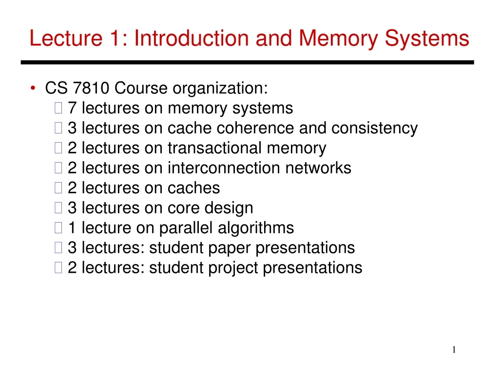
Lecture 1: Introduction and Memory Systems • CS 7810 Course organization: • 7 lectures on memory systems • 3 lectures on cache coherence and consistency • 2 lectures on transactional memory • 2 lectures on interconnection networks • 2 lectures on caches • 3 lectures on core design • 1 lecture on parallel algorithms • 3 lectures: student paper presentations • 2 lectures: student project presentations
Logistics • Reference texts: Parallel Computer Architecture, Culler, Singh, Gupta (a more recent reference is Fundamentals of Parallel Computer Architecture, Yan Solihin) Principles and Practices of Interconnection Networks, Dally & Towles Introduction to Parallel Algorithms and Architectures, Leighton Memory Systems: Cache, DRAM, Disk, Jacob et al. A number of books in the Morgan and Claypool Synthesis Lecture series
More Logistics • Projects: simulation-based, creative, teams of up to 4 students, be prepared to spend time towards middle and end of semester – more details in a few weeks • Final project report due in late April (will undergo conference-style peer reviewing); also watch out for workshop deadlines for ISCA • One assignment on memory scheduling due in early Feb • Grading: • 50% project • 20% assignment • 10% paper presentation • 20% take-home final
DRAM Main Memory • Main memory is stored in DRAM cells that have much higher storage density • DRAM cells lose their state over time – must be refreshed periodically, hence the name Dynamic • DRAM access suffers from long access time and high energy overhead • Since the pins on a processor chip are expected to not increase much, we will hit a memory bandwidth wall
Memory Architecture Processor Bank Row Buffer Memory Controller Address/Cmd DIMM Data • DIMM: a PCB with DRAM chips on the back and front • Rank: a collection of DRAM chips that work together to respond to a request and keep the data bus full • A 64-bit data bus will need 8 x8 DRAM chips or 4 x16 DRAM chips or.. • Bank: a subset of a rank that is busy during one request • Row buffer: the last row (say, 8 KB) read from a bank, acts like a cache
DRAM Array Access 16Mb DRAM array = 4096 x 4096 array of bits 12 row address bits arrive first Row Access Strobe (RAS) 4096 bits are read out Eight bits returned to CPU, one per cycle 12 column address bits arrive next Column decoder Column Access Strobe (CAS) Row Buffer
Salient Points I • DIMM, rank, bank, array form a hierarchy in the storage organization • Because of electrical constraints, only a few DIMMs can be attached to a bus • Ranks help increase the capacity on a DIMM • Multiple DRAM chips are used for every access to improve data transfer bandwidth • Multiple banks are provided so we can be simultaneously working on different requests
Salient Points II • To maximize density, arrays within a bank are made large rows are wide row buffers are wide (8KB read for a 64B request) • Each array provides a single bit to the output pin in a cycle (for high density and because there are few pins) • DRAM chips are described as xN, where N refers to the number of output pins; one rank may be composed of eight x8 DRAM chips (the data bus is 64 bits) • The memory controller schedules memory accesses to maximize row buffer hit rates and bank/rank parallelism
Salient Points III • Banks and ranks offer memory parallelism • Row buffers act as a cache within DRAM • Row buffer hit: ~20 ns access time (must only move data from row buffer to pins) • Empty row buffer access: ~40 ns (must first read arrays, then move data from row buffer to pins) • Row buffer conflict: ~60 ns (must first writeback the existing row, then read new row, then move data to pins) • In addition, must wait in the queue (tens of nano-seconds) and incur address/cmd/data transfer delays (~10 ns)
Technology Trends • Improvements in technology (smaller devices) DRAM capacities double every two years, but latency does not change much • Power wall: 25-40% of datacenter power can be attributed to the DRAM system • Will soon hit a density wall; may have to be replaced by other technologies (phase change memory, STT-RAM) • The pins on a chip are not increasing bandwidth limitations
Power Wall • Many contributors to memory power (Micron power calc): • Overfetch • Channel • Buffer chips and SerDes • Background power (output drivers) • Leakage and refresh
Power Wall • Memory system contribution (see HP power advisor): IBM data, from WETI 2012 talk by P. Bose
Overfetch • Overfetch caused by multiple factors: • Each array is large (fewer peripherals more density) • Involving more chips per access more data transfer pin bandwidth • More overfetch more prefetch; helps apps with locality • Involving more chips per access less data loss when a chip fails lower overhead for reliability
Selective Bitline Activation • Additional logic per array so that only relevant bitlines are read out • Essentially results in finer-grain partitioning of the DRAM arrays • Two papers in 2010: Udipi et al., ISCA’10, Cooper-Balis and Jacob, IEEE Micro
Rank Subsetting • Instead of using all chips in a rank to read out 64-bit words every cycle, form smaller parallel ranks • Increases data transfer time; reduces the size of the row buffer • But, lower energy per row read and compatible with modern DRAM chips • Increases the number of banks and hence promotes parallelism (reduces queuing delays) • Initial ideas proposed in Mini-Rank (MICRO 2008) and MC-DIMM (CAL 2008 and SC 2009)
DRAM Variants – LPDRAM and RLDRAM • LPDDR (low power) and RLDRAM (low latency) Data from Chatterjee et al. (MICRO 2012)
LPDRAM • Low power device operating at lower voltages and currents • Efficient low power modes, fast exit from low power mode • Lower bus frequencies • Typically used in mobile systems (not in DIMMs)
Heterogeneous Memory Chatterjee et al., MICRO 2012 • Implement a few DIMMs/channels with LPDRAM and a few DIMMs/channels with RLDRAM • Fetch critical data from RLDRAM and non-critical data from LPDRAM • Multiple ways to classify data as critical or not: • identify hot (frequently accessed) pages • the first word of a cache line is often critical Every cache line request is broken into two requests
Title • Bullet