Download
1 / 13
130 likes | 365 Views
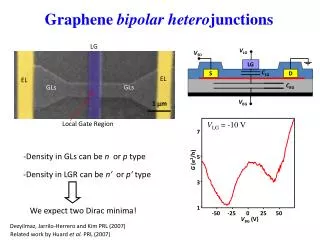
7. 5. G (e 2 /h). V LG = -10 V. 3. 1. -50. -25. 0. 25. 50. V BG (V). We expect two Dirac minima!. Graphene bipolar hetero junctions. LG. V LG. V SD. LG. C LG. S. D. EL. EL. C BG. GLs. GLs. V BG. 1 m m. Local Gate Region. -Density in GLs can be n or p type.

E N D
7 5 G (e2/h) VLG = -10 V 3 1 -50 -25 0 25 50 VBG (V) We expect two Dirac minima! Graphene bipolar heterojunctions LG VLG VSD LG CLG S D EL EL CBG GLs GLs VBG 1 mm Local Gate Region -Density in GLs can be n or p type -Density in LGR can be n’ or p’ type Oezyilmaz, Jarrilo-Herrero and Kim PRL (2007) Related work by Huard et al. PRL (2007)
G (e2/h) 50 2 4 6 8 10 12 25 potential x VBG (V) 0 n-p’-n n-n’-n 1 mm -25 -50 potential p-p’-p p-n’-p x 10 -10 -5 0 5 VLG (V) 7 potential x 5 G (e2/h) n p p n n p p’ n p p n’ n 3 potential 1 x -50 -25 0 25 50 VBG (V) Graphene heterojunction Devices p p n’
Klein Tunneling Transmission coefficient Ttot f potential x np=1x1012 cm2 n p n np=3x1012 cm2 nn=0.5x1012 cm2 Ballistic Quantum Transport in Graphene Heterojunction Novoselov et al, Nat. Phys (2006) Graphene NPN junctions Collimation: (resonance) k2x = pn/L Perfect transmission
electrode Smooth electrostatic n ~ 1012 cm-2 lF ~ 30 nm ddielectric ~ 20 nm L ~ 100 nm graphene transmission T Tunneling through smooth pn junction 1 mm f SEM image of device Cheianov and Fal’ko (2006) Zhang and Fogler (2008) Mean free path ~ 50 nm Tunneling through Classically Forbidden regime 20 nm T Realistic Graphene Heterojunction Requirements for Ballistic pn junctions Mean free path < 100 nm • Long Mean free path • -> Ballistic conduction • Large electric field -> • Small d -> • promote resonance Strong forward Collimation!
Transport Ballistic Graphene Heterojunction 12 electrode nnn ppp graphene 10 8 PN junction resistance npn Conductance (mS) pnp Cheianov and Fal’ko (‘06) 1 mm 6 Conductance Oscillation: Fabry-Perot n1,, k1, T T 4 R 18 V n2,, k2 L q´ R* T -18 V n1,, k1, -10 -8 -6 -4 -2 0 0 2 4 6 8 10 q VTG (V) k1 /k2= sinq’/ sinq Df= 2L /cosq’ Young and Kim (2008) VBG = 90 V VBG =-90 V See also Shavchenko et al and Goldhaber-Gordon’s recent preprint
Quantum Oscillations in Ballistic Graphene Heterojunction n1,, k1, Magnetoresistance Oscillations (B=0) T T R n2,, k2 L dR/dntop ( h/e2 10-15 cm-2) q´ R* T n1,, k1, q FB 5 FB=B L2 sinq ’/cosq ’ Aharonov-Bohm phase: nback (1012 cm2) 2 1 -1 0 dG/dntop (e2/h10-15 cm-2) 0 0 B (T) -2 1 0 2 4 6 8 10 0 -1 -5 VT (V) ntop (1012 cm2) -5 0 5 Resistance Oscillations (VB=-50 V) )
Ballistic pn junction Exp • Collimation Theory Resonant Magneto-Oscillations in Graphene Heterojunctions See also Shytoy et al., arXiv:0808.0488 Two fitting parameters: lLGR = 27 nm; lGL= 50 nm
Graphene quantum dot Band gap engineered Graphene nanoribbons FET (Manchester group) Nonconventional Devices Graphene Veselago lense Graphene psedospintronics Graphene Spintronics Son et al.Nature (07) Cheianov et al.Science (07) Trauzettel et al.Nature Phys. (07) Graphene Electronics Conventional Devices Many body & correlated effect to come!
Conclusions • Carbon nanotube FET is mature technology demonstrating substantial improvement over Si CMOS • Controlled growth and scaling up of CNTFET remains as a challenge • Graphene provides scaling up solution of carbon electronics with high mobility • Controlled growth of graphene and edge contol remains as a challenge • Novel quantum device concepts have been demonstrated on graphene and nanontubes
Kim Group Picnic: 2008 Central Park, New York Acknowledgement Meninder Purewal (nanotube) Kirill Bolotin (suspended graphene) Melinda Han (nanoribon) Dmitri Efetov (graphene heterojuncton) Andrea Young (graphene heterojunction) Barbaros Oezyilmaz (now at NSU) Pablo Jarrilo-Herrero (now at MIT) Collaboration: Horst Stormer Funding:
100 W = 37 nm 10 Conductance (mS) d: dimensionality 4K 15K 1 100K 200K 300K Arrhenius plot 2D VRH 1D VRH 0.1 15 nm 15 nm 15 nm 22 nm 22 nm 22 nm 0 20 40 60 3 Vg (V) 31 nm 31 nm 31 nm 2 37 nm 37 nm 37 nm ln(R) ln(R) 1 ln(R) 48 nm 48 nm 48 nm 0 -1 70 nm 70 nm 70 nm -2 0.0 0.1 0.2 T-1/2 T-1/3 T-1 Variable Range Hopping in Graphene Nanoribbons E EF T x
LG EL EL GLs GLs 1 mm Local Gate Region simple model (following Haug et al) Graphene Quantum Hall Edge State Conduction Oezyilmaz, et al., PRL (2007) See also Related work by Williams et al. Science (2007)
12 nnn VBG = 90 V 10 8 npn Conductance (mS) 6 4 18 V -10 -8 -6 -4 -2 0 VTG (V) Temperature Dependent Oscillations