TRANSISTOR - Introduction
TRANSISTOR - Introduction. BIPOLAR JUNCTION TRANSISTOR (BJT). Introduction. Beside diodes, the most popular semiconductor devices is transistors. Eg: Bipolar Junction Transistor (BJT) Transistors are more complex and can be used in many ways

TRANSISTOR - Introduction
E N D
Presentation Transcript
TRANSISTOR - Introduction BIPOLAR JUNCTION TRANSISTOR (BJT)
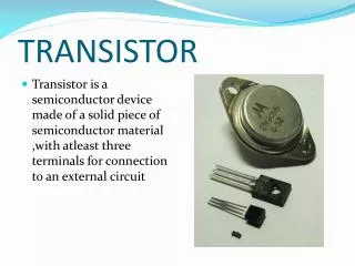
Introduction • Beside diodes, the most popular semiconductor devices is transistors. Eg: Bipolar Junction Transistor (BJT) • Transistors are more complex and can be used in many ways • Most important feature: can amplify signals and as switch • Amplification can make weak signal strong (make sounds louder and signal levels greater), in general, provide function called Gain
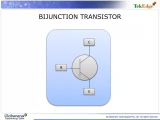
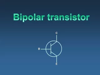
Transistor Structure • BJT is bipolar because both holes (+) and electrons (-) will take part in the current flow through the device • N-type regions contains free electrons (negative carriers) • P-type regions contains free holes (positive carriers) • 2 types of BJT • NPN transistor • PNP transistor • The transistor regions are: • Emitter (E) – send the carriers into the base region and then on to the collector • Base (B) – acts as control region. It can allow none,some or many carriers to flow • Collector (C) – collects the carriers
PNP and NPN transistor structure P N P N P N Ic(mA) IC(mA) IB(µA) IB(µA) IE(mA) IE(mA) Arrow shows the current flows
The collector is lightly doped. C The base is thin and is lightly doped. B E The emitter is heavily doped. NPN Transistor Structure N P N
Transistor configuration • Transistor configuration –is a connection of transistor to get variety operation. • 3 types of configuration: • Common Collector. • Common Base. • Common Emitter
Common-Collector Configuration • The input signal is applied to the base terminal and the output is taken from the emitter terminal. • Collector terminal is common to the input and output of the circuit • Input – BC • Output – EC • Input = Output
Common-Base Configuration • Base terminal is a common point for input and output. • Input – EB • Output – CB • Not applicable as an amplifier because the relation between input current gain (IE) and output current gain (IC) is approximately 1
Common-Emitter Configuration • Emitter terminal is common for input and output circuit • Input – BE • Output – CE • Mostly applied in practical amplifier circuits, since it provides good voltage, current and power gain
The C-B junction is reverse biased. NPN Transistor Bias No current flows. C N B P N E
The B-E junction is forward biased. NPN Transistor Bias C N B P N E Current flows.
Current flows everywhere. NPN Transistor Bias IC C N B P When both junctions are biased.... IB N E Note that IB is smaller than IE or IC. IE
IC Note: when the switch opens, all currents go to zero. C N Although IB is smaller it controls IE and IC. B P IB N E Gain is something small controlling something large (IB is small). IE
IC = 99 mA The current gain from base to collector is called b. C IB = 1 mA B P 99 mA IC N E b = = 99 IB 1 mA IE = 100 mA
IC = 99 mA Kirchhoff’s current law: C IB = 1 mA B P IE = IB + IC 99 mA = 1 mA + N E = 100 mA IE = 100 mA
IC = 99 mA In a PNP transistor, holes flow from emitter to collector. C IB = 1 mA B Notice the PNP bias voltages. E IE = 100 mA
Collector C Base B E Emitter NPN Schematic Symbol Memory aid: NPN means Not Pointing iN.
Collector C Base B E Emitter PNP Schematic Symbol
Fundamental operation of pnp transistor and npn transistor is similar except for: role of electron and hole, voltage bias polarity, and Current direction Recall: NPN and PNP Bias
I-V Characteristic for CE configuration : Input characteristic • Input characteristic: input current (IB) against input voltage (VBE) for several output voltage (VCE) • From the graph • IB = 0 A VBE < 0.7V (Si) • IB = value VBE > 0.7V (Si) • The transistor turned on when VBE = 0.7V
I-V Characteristic for CE configuration : Output characteristic • Output characteristic: output current (IC) against output voltage (VCE) for several input current (IB) • 3 operating regions: • Saturation region • Cut-off region • Active region
I-V Characteristic for CE configuration : Output characteristic • Saturation region – in which both junctions are forward-biased and IC increase linearly with VCE • Cut-off region – where both junctions are reverse-biased, the IB is very small, and essentially no IC flows, IC is essentially zero with increasing VCE • Active region – in which the transistor can act as a linear amplifier, where the BE junction is forward-biased and BC junction is reverse-biased. IC increases drastically although only small changes of IB. • Saturation and cut-off regions – areas where the transistor can operate as a switch • Active region – area where transistor operates as an amplifier
Current Relationships • Relations between IC and IE : α = IC IE • Value of αusually 0.9998 to 0.9999, α≈ 1 • Relations between IC and IB : β = IC@ IC = βIB IB • Value of β usually in range of 50 400 • The equation, IE =IC + IB can also written in β IC = βIB IE = βIB + IB => IE = (β + 1)IB • The current gain factor , α and β is: α =β @ β =α . β + 1α - 1