Download
1 / 43
430 likes | 585 Views
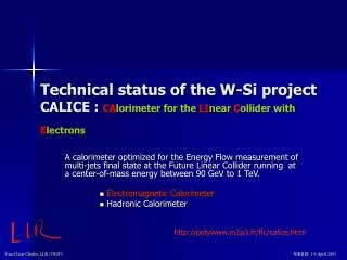
Technical status of the W-Si project CALICE : CA lorimeter for the LI near C ollider with E lectrons. A calorimeter optimized for the Energy Flow measurement of multi-jets final state at the Future Linear Collider running at a center-of-mass energy between 90 GeV to 1 TeV.

E N D
Technical status of the W-Si project CALICE : CAlorimeter for the LInear Collider with Electrons A calorimeter optimized for the Energy Flow measurement of multi-jets final state at the Future Linear Collider running at a center-of-mass energy between 90 GeV to 1 TeV. Electromagnetic Calorimeter Hadronic Calorimeter http://polywww.in2p3.fr/flc/calice.html
General view of the calorimeter Tracker : TPC ECAL : Sandwich Wplate & Si Wafer HCAL : DHCAL or AHCAL Coil : 4 T (2 )
ECAL concept : • A fine granularity calorimeter with large number of segmentation is proposed as the best solution for the energy flow, lepton identification, photon reconstruction with good precision on energy and direction. • On the other side, the coil thickness is bigger than usual due to the 4 Tesla field needed to maintain the machine background close to the beam pipe. Therefore , the ECAL has to be very compact. (1,30 m for ECAL and HCAL) • Such a calorimeter could be made of Tungsten-Silicon sandwich. • With pad of 1x1 cm and 40 layers : A TRACKER CALORIMETER . • It gives a clean picture of all energy flow objects in all type of events • Simulation using GEANT4 lead to think of an energy resolution on electron/photon in the region of Delta E /E = 11% / sqrt(E)
Prototypes overview Global view of the test beam setup VME/… ECAL general view HCAL 2nd structure (2×1.4mm of W plates) 3rd structure (3×1.4mm of W plates) 180 mm BEAM ECAL Beam monitoring Movable table VFE 370 mm 1st structure (1.4mm of W plates) 370 mm Detector slab Silicon wafer
Mould for alveolus structure 1.4 Structure 5 alveolus :(10 layers) Detector slab (here it is just a type H structure) Alveolus structures Design and construction of a mould with all metallic pieces for the 3 different structures
Sizes of the structure : Alveolus 374.5 mm 125.6 mm 8.5 mm
Front End electronics Shielding PCB Silicon wafer (Cfi / W) structuretype H Detector slab Transverseview Silicon wafer (0.525 mm) PCB (multi-layers) ( 2.4 mm) Al. Shielding 8.5 mm • PCB : • 14 layers • Thickness 2.4 mm Composite structure(0.15 mm / layer) Tungsten (1.4 mm, 2×1.4 or 3×1.4 mm)
Carbon fiber Tungsten 1.4 mm thick Type H structure Conception and realization of mould for manufacturing the whole 30 typeH structures (3 different thickness W) : Ended alveolar : Mould structure H :
Sizes of the structure : Slab Aluminum foil : ~0.1 mm PCB : 2.4 mm Wafer : 0.525 mm Carbon fiber : 0.15 mm 8,3 mm W plate : 1.4 mm
PCB, Wafer, Chip : still in progress PCB Wafer
PCB, Wafer, Chip : still in progress PCB Chip
ECAL prototype silicon wafer description • 4” high resistivity wafers • 525 microns thick – 5Kcm • tile side: 62.0 + 0.0 • - 0.1 mm • guard ring Dead zone width is only 1mm First test production with 43 wafers 39 good (< 2 nA leakage)
Wafer : Thickness : 525 microns 3 % In silicon ~80 e-h pairs / micron 42000 e- /MiP Capacitance : ~25 pF Leakage current : 1 – 5 nA Full depletion bias : ~150 V Nominal operating bias : 200 V Institute of Nuclear Physics - Moscow State University Institute of Physics, Academy of Sciences of the Czech Republic - Prague Leakage curent (nA)
2 2 2 2 2 62mm 10mm 6 2 10mm Diode footprint 62mm 1 wafer Diode bias Sig. readout Diode pin out Detector schematic description Amorphous silicon deposition Resistance Capacitance(AC coupling) Yvan Bonnasieux Physique des Interfaces et Couches Minces - Ecole Polytechnique - Palaiseau Aluminium sheet PCB Wafers The aluminium sheet is the ground
Passive component on the wafer : • Capacitance : • Dielectric : silicon nitrite • Refractive index : n=2 • Thickness : e = 2 m C= 1,32 nF • Resistance : • material : aSiH • Resistivity : =1011 .cm • Thickness : l = 2 m R= 102 M
Passive component on the wafer : • Capacitance : C ~ 1.4 nF Leakage current Problemof measurement • Resistance : Still in progress …
Gluing of Si wafer A automatic device is use to deposit the conductive glue : Gluing and placement ( 0.1 mm) of270wafers with 6×6 pads About 10 000 points of glue. X-Y-Z table (400×400×150 mm3) with glue dispensing tool (conductive glue)
Charge preamp Detector shaper Track & hold Vdc = -200V Amp DC block OPA Front end electronic : Asic Laboratoire de l'Accélérateur Linéaire - Orsay
Charge preamp Detector shaper Track & hold Vdc = -200V Amp DC block OPA Front end electronic : Asic Laboratoire de l'Accélérateur Linéaire - Orsay 4.2 pC max input charge (650 MIP) 2.8V dynamic range below 1% non-linearity
Charge preamp Detector shaper Track & hold Vdc = -200V Amp DC block OPA 180nspeaking time Front end electronic : Asic Laboratoire de l'Accélérateur Linéaire - Orsay
Charge preamp Detector shaper Track & hold Vdc = -200V Amp DC block OPA Front end electronic : Asic Laboratoire de l'Accélérateur Linéaire - Orsay Multiplexing output : 18 channel / chip 2 chips / wafer ENC = 2200 @ 80 pF Talk from Bernard Bouquet : R&D for ECAL-VFE technology prototype
Linearity simulation New FLC_PHY2 • Peaking time is 200ns on both gain • High-gain shapers can be shut down by switching off their biases • Two different output for low gain and high gain • Interface compatibility with the read out is kept New interface not written at this point Transient simulation
DAQ :VME (use and modify CMS board for Si tracker) Need of 6 boards for physic prototype Talk from Paul Dauncey : DAQ for the CALICE beam test
Cosmic test bench: general view • 2 XY planes : 16 in X et 16 in Y (40x40 cm2) • scintillators reading : PM + Ampli + Trigger Logic • Crate VME : • QDC CAEN • Trigger + Veto (dual timer) • Crate Controller : PCI MXI-2 (NI) board
Cosmic test bench: general view • Pattern generation board (Labo) : • Numerical CPLD • Clock toward PCB : 208 KHz • Level translator TTL/RS422
Cosmic test bench: general view Commercial board (National Instrument) - PCI Interface - ADC 12 bits (1.25 Msa/s) - DMA Transfer - Input dynamic : from +/- 0.05 to +/- 10V Talk from Cristina Lo Bianco : Assembly and cosmic test for the W-SI prototype (CALICE)
Other ECAL R&D • Thermal studies • VFE inside beam(Chip evaluation board and small DAQ are ready) • Passive component on the wafer (Capacitance Ok and resistance still in progress) • Amorphous silicon … (works of Pierre Jarron at Cern) • …
Other ECAL R&D • Thermal studies
Other ECAL R&D • Thermal studies In the case of 40 layers and considering a power dissipated of about 5 mW/cm2 the temperature at the middle of structure would be about 280 °C
Cooling channel Heat points (VFE chip) Thermal sensors Externalconnections PCB 1mm thick(with wafers) Structure type H Radiator aluminium plate Other ECAL R&D • Thermal studies
Other ECAL R&D • Thermal studies • VFE inside beam(Chip evaluation board and small DAQ are ready) • Passive component on the wafer (Capacitance Ok and resistance still in progress) • Amorphous silicon … (works of Pierre Jarron at Cern) • …
Physic prototype : who ? • Mechanic : • W plates : Russian • ECAL Structure : LLR • Infrastructure of beam test : LPC Clermont-ferrand ? and ? • beam Hodoscope : ? • Data processing : • DAQ / Event Builder : ? • Simulation : LLR • Electronic : • VFE : LAL • DAQ : UK • Slow control : ? • Instrumentation : • silicon : LLR and PICM + Russian and Czech • ECAL Integration :LLR • Cosmic test bench : LLR
Conclusion : • Physic prototype program is well advances • First test beam with electrons mi 2004 • First hadronic test beam 2005 • All is not covered : • Physic prototype in 2004 • R&D (thermal et electronic) • … http://polywww.in2p3.fr/flc/calice.html