Understanding CPU Design: Single-Cycle and Multi-Cycle Architectures
210 likes | 342 Views
This lecture covers fundamental CPU design concepts, focusing on performance factors such as instruction count, CPI, and cycle time. We will explore two MIPS implementations: a simplified single-cycle CPU and a more realistic pipelined version. Key topics include instruction execution through the program counter, the role of ALUs in arithmetic operations, and the use of multiplexers in data pathways. We'll also discuss various instruction types including load/store and control transfer, and highlight the construction of a MIPS datapath, emphasizing combinational and sequential logic elements in CPU architecture.

Understanding CPU Design: Single-Cycle and Multi-Cycle Architectures
E N D
Presentation Transcript
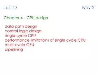
Lec 17 Nov 2Chapter 4 – CPU designdata path design control logic design single-cycle CPU performance limitations of single cycle CPU multi-cycle CPU pipelining
Introduction §4.1 Introduction • CPU performance factors • Instruction count • Determined by ISA and compiler • CPI and Cycle time • Determined by CPU hardware • We will examine two MIPS implementations • A simplified version • A more realistic pipelined version • Simple subset, shows most aspects • Memory reference: lw, sw • Arithmetic/logical: add, sub, and, or, slt • Control transfer: beq, j
Instruction Execution • PC instruction memory, fetch instruction • Register numbers register file, read registers • Depending on instruction class • Use ALU to calculate • Arithmetic result • Memory address for load/store • Branch target address • Access data memory for load/store • PC target address or PC + 4
Multiplexers • Can’t just join wires together • Use multiplexers
An ALU for MicroMIPS A multifunction ALU with 8 control signals (2 for function class, 1 arithmetic, 3 shift, 2 logic) specifying the operation.
Logic Design Basics • Information encoded in binary • Low voltage = 0, High voltage = 1 • One wire per bit • Multi-bit data encoded on multi-wire buses • Combinational element • Operate on data • Output is a function of input • State (sequential) elements • Store information §4.2 Logic Design Conventions
A Y B A A Mux I0 Y + Y Y I1 ALU B B S F Combinational Elements • AND-gate • Y = A & B • Adder • Y = A + B • Arithmetic/Logic Unit • Y = F(A, B) • Multiplexer • Y = S ? I1 : I0
D Q Clk Clk D Q Sequential Elements • Register: stores data in a circuit • Uses a clock signal to determine when to update the stored value • Edge-triggered: update when Clk changes from 0 to 1
Clocking Methodology • Combinational logic transforms data during clock cycles • Between clock edges • Input from state elements, output to state element • Longest delay determines clock period
Building a Datapath • Datapath • Elements that process data and addressesin the CPU • Registers, ALUs, mux’s, memories, … • We will build a MIPS datapath incrementally • Refining the overview design §4.3 Building a Datapath
Instruction Fetch Increment by 4 for next instruction 32-bit register
R-Format Instructions • Read two register operands • Perform arithmetic/logical operation • Write register result
Load/Store Instructions • Read register operands • Calculate address using 16-bit offset • Use ALU, but sign-extend offset • Load: Read memory and update register • Store: Write register value to memory
Branch Instructions • Read register operands • Compare operands • Use ALU, subtract and check Zero output • Calculate target address • Sign-extend displacement • Shift left 2 places (word displacement) • Add to PC + 4 • Already calculated by instruction fetch • Compiler computes the offset as (current address – target address – 4).
Branch Instructions Justre-routes wires Sign-bit wire replicated
Composing the Elements • First-cut data path executes an instruction in one clock cycle • Each datapath element can only do one function at a time • Hence, we need separate instruction and data memories • Use multiplexers where alternate data sources are used for different instructions


