16°
Crack development in lead-free solder in PGBA package due to recrystallization that forms ‘red’ orientations Thomas R. Bieler , Michigan State University, DMR 1006656. SAC 305 lead-free solder joints on PBGA package pre-aged 100° C/500hrs 6400 0~100 °C thermal cycles.

16°
E N D
Presentation Transcript
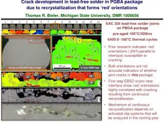
Crack development in lead-free solder in PGBA packagedue to recrystallization that forms ‘red’ orientationsThomas R. Bieler, Michigan State University, DMR 1006656 SAC 305 lead-free solder joints on PBGA package pre-aged 100°C/500hrs 6400 0~100°C thermal cycles • Prior research indicates ‘red’ orientations ( [001] parallel to interface) susceptible to cracking • Bulk orientations are not accurate indicators of whether joint cracks in this package. • Fine step EBSD scans near interface show ‘red’ orientations highly correlated with cracking resulting from continuous recrystallization. • Mechanism of continuous recrystallization depends on activated slip systems that will be analyzed in the coming year C-axis OIM map Cross-polarized light image 21° 42° 17° 18° 16° 18° 14° 52° 48°
In-situ synchrotron X-ray characterization of lead-free solder;melting, dissolution and resolidification kinetics are quantified…Thomas R. Bieler, Michigan State University, DMR 1006656 SAC-305 lead-free solder balls in a Wafer-Level-Chip-Scale package Integrated diffraction patterns from ball and interface metallurgy 806.5 s ~219°C 810 s ~224°C Sn Cu6Sn5 (a) (b) Ag3Sn Ni3Sn4 Cu • (a)(b): Melting process; • (c)(d): Resolidification • Melting and solidification occurs in about 0.5-1s, but complete melting of Sn and dissolution of IMCs can take 3-30 seconds. • Cu6Sn5 IMC remains with no dramatic change during the melting and solidification process. • Co-existence of molten Sn and earliest formed Sn nuclei are evident in (c, d, arrows). • Each reflow results in different crystal orientations, (a) vs. (d). • First proof of what has been speculated by scientists and manufacturers for years Si Liquid Sn broad peak (101) (200) (211) (301) (321) (312) (110) (101) (113) (200) (220) (111,021) Liquid Sn broad peak Si (c) (d) 923s ~195°C 922.5s ~195°C

