Download
1 / 13
130 likes | 155 Views
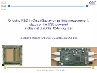
Ongoing R&D in Orsay/Saclay on ps time measurement: status of the USB-powered 2-channel 3.2GS/s 12-bit digitizer D.Breton & J.Maalmi (LAL Orsay), E.Delagnes (CEA/IRFU). Séminaire DRT/LIST 08/09/08 SACLAY. History of the Orsay/Saclay SCA Developments.

E N D
Ongoing R&D in Orsay/Saclay on ps time measurement: status of the USB-powered 2-channel 3.2GS/s 12-bit digitizerD.Breton & J.Maalmi (LAL Orsay), E.Delagnes (CEA/IRFU) Séminaire DRT/LIST 08/09/08 SACLAY.
History of the Orsay/Saclay SCA Developments • Story begins in 1992 with the first prototype of the SCA for the ATLAS LARG calorimeter. The final numbers of this rad-hard circuit: • 40 MHz sampling • 13.6 bits Dynamic Range with simultaneous write/read • 80000 chips produced in 2002 and mounted on the detector. • Since then, 3 new models of fast samplers have been designed (>30000 chips in use). • Design philosophy: • 1. Maximize dynamic range and minimize signal distorsion. • 2. Minimize need for calibrations and off-chip data corrections. • 3. Minimize costs (both for development & production): • Use of inexpensive CMOS technologies (0.8µm then 0.35µm); • Use of packaged chips (cheap QFP).
Top Read Bus Vout=A / (1+A) * Q/Cs =V1 * A/(1+A) Bottom Read BUS 4 Cs Write Bus N capacitors 3 N capas v V1=V Q=Cs.V1 2 1 Return Bus Main Common design options (1): • 4-switch memory cells: • Voltage-mode writing. • Floating voltage-mode reading with read amplifier. • Gain and pedestal spread insensitive to capacitor mismatches. • Sequencing of S1-S2 switch opening. • Sampling time very well defined and independent of signal amplitude. • Use of analog input buffer (voltage follower): • Keeps the real input impedance very high to avoid signal distortion • Penalty in power consumption and bandwidth.
Main Common design options (2): • Relatively high value of storage capacitance (200fF to 1pF): • minimize both kt/C and readout noise. • Use of differential channels: • Easier interface with modern commercial ADCs. • Low signal distortion • Noise rejection • Use of internally servo-controlled Delay Lines (DLL) to define the time steps: • No need for timing calibration. • Stability with temperature. • While on-chip phase detector and charge pump, fast setup time for the servo-control is possible: sampling DLL
The Sampling Matrix Structure: main features • Short DLL: • smaller jitter. • small timing non-linearity • 1 servo control of Delay / Col => high stability. • Analog bus split in divisions (lines) => shorter analog bus • More uniform bandwidth. • Less analog delay along the bus.
The SAM (Swift Analog Memory) chip • 2 differential channels • 256 cells/channel • BW > 500 MHz • Sampling Freq 400MHz->3.2GHz • High Readout Speed > 16 MHz • Smart Read pointer (integrates a 1/Fs step TDC) • Few external signals • Many modes configurable by a serial link. • Auto-configuration @ power on • AMS 0.35 µm => low cost for medium size prod NIM A, Volume 567, Issue 1, p. 21-26, 2006 6000 ASICs manufactured, tested and delivered in Q2 2007
The USB_WaveCatcher prototype board Reference Clock: 200MHz => 3.2GS/s Power consumption < 2.5W Pulsers for reflectometry applications 1 GHz BW amplifier. µ USB Trigger input 2 analog inputs. DC coupled Trigger output Trigger discriminators Dual 12-bit ADC SAM Chip
-3dB 530 MHz Examples of acquisitions: no off-line correction Channel 0 Channel 1 Channel 0 Channel 1 2ns FWHM consecutive pulses, separated by 22ns , (300mV & 170mV amplitude). 3.2 GS/s 75 mV amplitude, 1ns FWHM pulse. 3.2GS/s Bode plot for 300mV pp Sinus
Fixed pattern jitter • DNL => modulo 16 pattern = 6.6 ps rms => ~0.5ps after correction. After correction DNL After correction INL • INL => modulo 16 pattern + slow pattern = 16 ps rms => ~1ps after correction. • Position correlated => can be corrected by software • Advantage of servo-controlled structure: very small dependence to time and temperature
Random jitter • With random trigger: jitter floor ~ 2.2 ps rms • A little more jitter on “transition” samples (3.5 ps). • Understood: due to the clock jitter which can be seen only on the last cell of the DLLs • => Mean jitter ~ 2.5 ps rms
Towards the cosmic telescope @ SLAC • We started designing a version of the board compatible with the MCPPMT equipped part of the SLAC cosmic telescope • It will house channels of analog memory and an USB 480Mbits/s interface • We will also develop the acquisition software with LabWindows/CVI • The time target is fall of this year
R&D on a ps TDC in IBM 130nm technology • We are collaborating to the design of a new TDC in the IBM 130nm technology • This is a collaboration between Orsay, Saclay, and the University of Chicago (with the help of Gary Varner). • The goal is to reach the ps precision thanks to the addition to an usual DLL based TDC of analog memories sampling at very high frequency (20GS/s). • Input clock frequency should be 312.5 MHz • The design of the first prototype is well on tracks • It will include a complete measurement channel • Main elements are designed now, except the fast discriminator • In the near future, we aim at building a 16-channel chip with integrated output buffers. • These chips will be used at the output of fast PMT’s • We already have a SiPM test bench here at LAL driven by the “instrumentation” group • This bench will soon be extended to MCPPMT’s
Conclusion • We built a USB board to push the SAM chip towards its limits. • Timing measurements showed a timing resolution of ~16 ps rms without time INL correction, and a few ps after correction. • The board will be tested with MCPPMT’s. • There are still some points to understand (strange modulo 4 effect appears on time INL after power cycling: seems to come from FPGA …) => but the next version of the board is ready to leave. • Tests gave us new guidelines for future chips to improve timing performances. • We are now convinced that a single chip can’t be optimum for all applications (long depth vs time precision). • Next circuit will be submitted in July: 32 channels, 5GS/s sampling freq, larger BW (700MHz ?), same techno (0.35µm), larger depth (512 pts/ch) • Then an upgraded version of SAM will be designed • target = precision time measurement • We started designing a board for the cosmic telescope at SLAC • A new ps TDC using ultra-fast analog memories is under design.