Download

1 / 36
370 likes | 544 Views
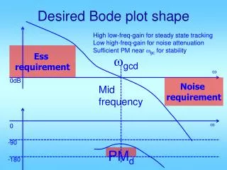
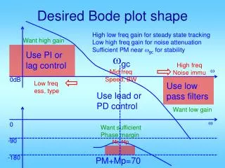
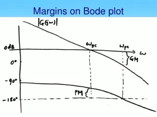
Desired Bode plot shape. High low freq gain for steady state tracking Low high freq gain for noise attenuation Sufficient PM near w gc for stability. Want high gain. Use PI or lag control. w gc. High freq Noise immu. w. Mid freq Speed, BW. 0dB. Low freq ess , type.

E N D
Desired Bode plot shape High low freq gain for steady state tracking Low high freq gain for noise attenuation Sufficient PM near wgc for stability Want high gain Use PI or lag control wgc High freq Noise immu w Mid freq Speed, BW 0dB Low freq ess, type Use low pass filters Use lead or PD control Want low gain w 0 Want sufficient Phase margin -90 Mr, Mp -180 PM+Mp=70
Overall Loop shaping strategy • Determine mid freq requirements • Speed/bandwidth wgc • Overshoot/resonance PMd • Use PD or lead to achieve PMd@ wgc • Use overall gain K to enforce wgc • PI or lag to improve steady state tracking • Use PI if type increase neede • Use lag if ess needs to be reduced • Use low pass filter to reduce high freq gain
Proportional controller design • Obtain open loop Bode plot • Convert design specs into Bode plot req. • Select KP based on requirements: • For improving ess: KP = Kp,v,a,des / Kp,v,a,act • For fixing Mp: select wgcd to be the freq at which PM is sufficient, and KP = 1/|G(jwgcd)| • For fixing speed: from td, tr, tp, or ts requirement, find out wn, let wgcd= (0.65~0.8)*wn and KP = 1/|G(jwgcd)|
PD control design Variation • Restricted to using KP = 1 • Meet Mp requirement • Find wgc and PM • Find PMd • Let f = PMd – PM + (a few degrees) • Compute TD = tan(f)/wgcd • KP = 1; KD=KPTD
Lead Design • From specs => PMd and wgcd • From plant, draw Bode plot • Find PMhave = 180 + angle(G(jwgcd) • DPM = PMd - PMhave + a few degrees • Choose a=plead/zlead so that fmax = DPM and it happens at wgcd
Alternative use of lead • Select K so that KG(s) meet ess req. • Find wgc and PM, also find PMd • Determine phi_max, and alpha • Place phi_max a little higher than wgc
Lag and lead-lag Design Steps • From plant, draw Bode plot • From specs => PMd and wgcd • If there is speed or BW req, wgcd, • In this case, if PM not enough, design PD or lead • Otherwise, choose wgcd to have PM>PMd • Find K to enforce wgcd: • Find Kp,v,a-have with K and C above • Find Kp,v,a-des from ess specs • zlag/plag = Kp,v,a-des/Kp,v,a-have • Let zlag= wgcd/5~20, depending on PM room • Compute plag
Basic PI Design Steps • From plant, draw Bode plot • From specs => PMd and wgcd • If there is speed or BW req, wgcd, • In this case, if PM not enough, design PD or lead • Otherwise, choose wgcd to have PM>PMd • Find K to enforce wgcd: • Let KP = K • And KI = Kwgcd/5~20, depending on extra PM room to spare Need to increase type to make a nonzero ess to be zero. But no requirement on ess after type increase.
PI Design with ess specs • From plant, draw Bode plot • From specs => Kv,a-des, PMd and wgcd • For required ess, Kv,a-des =1/ess • With C(s)=1/s, compute Kv,a-have • If there is speed or BW req, wgcd, • In this case, if PM not enough, design PD or lead • Otherwise, choose wgcd to have PM>PMd • Find K to enforce wgcd: • Let KP = K, KIdes= Kv,a-des/Kv,a-have • If KIdes <= Kwgcd/5~20, done, let KI = KIdes • Else, increase wgcd and go back to previous step Need to increase type by 1 to make a nonzero ess to be zero, and after type increase, there is further requirement on ess.
PI Design with PD Design Steps • From required ess, Kv,a-des =1/ess • With C(s)=1/s, compute Kv,a-have • Let KI = Kv,a-des/Kv,a-have • Multiply G(s) by KI/s • Do a PD design for KIG(s)/s, with DC gain=1: • Find wgc and PM • Find PMd • Let f = PMd – PM + (a few degrees) • Compute TD = tan(f)/wgcd • KP = KI*TD
Alternative PI Design Steps • For required ess, Kv,a-des =1/ess • With C(s)=1/s, compute Kv,a-have • Let KI = Kv,a-des/Kv,a-have • Rewrite char eq: (KP + KI/s)G(s) + 1=0 • KP*n/d + KI*n/d/s +1 = 0 • KP *n*s + KI*n+d*s =0, KP*n*s/(KI*n+d*s) + 1 =0 • So do a KP design for n*s/(KI*n+d*s), with KI above • Draw Bode plot for n*s/(KI*n+d*s) • Select max PM frequency • Compute KP to make that frequency wgc
Two d.o.f. Control design C(s) Gp(s) d + r + e C1(s) Gp(s) y + _ _ C2(s) C1(s) = C(s) – C2(s)
Loop transfer function is still C(s)Gp(s) • TF from d to y: Gp(s)/(1+C(s)Gp(s)) • TF from r to y: C1(s)Gp(s)/(1+C1(s)Gp(s) +C2(s)Gp(s))=C1(s)Gp(s)/(1+C(s)Gp(s)) • Design C(s) to achieve desired loop shape • Split C(s) into C1 and C2 • Dual loop implementation to individually control disturbance TF and reference TF
Dual loop control to increase type • Recall: type with respect to r = #integrators in TF from e to where r enters • This = #integrator in C1 + #integrator in inner loop • Therefore, choose C2 so that #integrators in inner loop is more than #integrators in Gp(s) • Overall loop TF not affected • Input/output TF Poles not affected • Input/output TF Zeros affected • Steady state tracking improved
Inner loop TF • Not easy to see in this general form • But simply pick C2 to cancel one or two lowest order terms in Gp • See example
y _ C2(s) C2 = -2s Implement as: y _ -2
Example • Design problem from text book • But our solution is much more meaningful and much easier • Plant TF Gp(s) = 10/s(s+1) • Specs: • Mp <19%, but >2% • Ts <1 sec • Ess to step, ramp, acc all = 0
s=tf('s'); Gp=10/s/(s+1); figure; margin(Gp); grid; ts = 1; %specification t=linspace(0,3*ts,301); Gcl=Gp/(1+Gp); figure; step(Gcl,t); grid; %specification for Mp is 2% to 19% %can use the mid point as initial target Mp=10; zeta=0.6; %for Mp=10% sigma=4/ts; %no tolerance band is given, so use 2% wn=sigma/zeta; wgcd=0.7*wn; Gwgc = evalfr(Gp, j*wgcd); PM=angle(Gwgc)/pi*180 + 180;
PMd = 70 - Mp + 10; %add 10 deg because we need PI later DPM = PMd - PM; %phase margin deficiency z_PD = wgcd /tan(DPM*pi/180); %PD control K = 1/abs(evalfr((s+z_PD)*Gp,j*wgcd)); C=K*(s+z_PD); figure; margin(C*Gp); grid; %Bode with PD figure; step(C*Gp/(1+C*Gp),t); grid; %now add PI, place zero of PI at wgcd/10 %Mp target of 10% together with 10 deg extra PMd %can tolerate a little more phase delay from PI. z_PI = wgcd/10; C=C*(s+z_PI)/s; %multiply PI and PD figure; margin(C*Gp); grid; figure; step(C*Gp/(1+C*Gp),t); grid;
Step response after PD Ts is two large, need to increase wgc by 1.5X
wgc=0.7*wn*1.6; z_PI = wgc/20;
Wgc increased from 4.47 to 7.47 After PD
Ts is now about right After PD
After PID Ts is OK Mp is OK
PD +0.1s y PI _ _ -0.1 C2(s) = -0.1s
PI*PD +0.1s y _ _ -0.1
The 2 DOF implementation caused 5% additional overshoot. Increase PMd by 7 to target 15% Mp
… … Mp=10; zeta=0.6; %for Mp=10% sigma=4/ts; %no tolerance band is given, so use 2% wn=sigma/zeta; wgcd=0.7*wn*1.6; Gwgc = evalfr(Gp, j*wgcd); PM=angle(Gwgc)/pi*180 + 180; PMd = 70 - Mp + 17; %add 10 deg because we need PI later DPM = PMd - PM; %phase margin deficiency z_PD = wgcd /tan(DPM*pi/180); %PD control K = 1/abs(evalfr((s+z_PD)*Gp,j*wgcd)); C=K*(s+z_PD); … …. z_PI = wgcd/20; C=C*(s+z_PI)/s; %multiply PI and PD figure; margin(C*Gp); grid; figure; step(C*Gp/(1+C*Gp),t); grid; figure; step((C+0.1*s)*Gp/(1+C*Gp),t); grid;