Download
1 / 22
220 likes | 240 Views
SMU Activities Jingbo Ye May 9, 2005, CERN, for Opto-Electronics Readout Systems for SLHC. System and Irradiation Tests on the GOL chip. LoC (link on chip) development based on SoS technology. GOL chip.

E N D
SMU ActivitiesJingbo YeMay 9, 2005, CERN, for Opto-Electronics Readout Systems for SLHC. System and Irradiation Tests on the GOL chip. LoC (link on chip) development based on SoS technology.
GOL chip • GOL: 1.6 Gbps serializer + laser driver in one chip, 0.5m CMOS technology with radiation tolerant layout. Works with HDMP-1024 and TLK2501 as deserializer. • System tests carried out by CERN and experiments that plan to use this chip. • Irradiation tests so far: 10 Mrad(SiO2) with 10KeV X-rays, 3.14×10¹²p/cm2, 60MeV proton, no SEU observed.
System and Irradiation tests of the GOL chip planned at SMU • System test: • GOL clock jitter tolerance with HDMP-1024 or TLK2501 as deserializer. • GOL clock jitter conversion from the reference clock to the serial data stream. • GOL driving characteristics with a VCSEL and with an Edge Emitting Laser. • Irradiation test: • 200 MeV proton with fluences up to 1015 – 1016 p/cm2. • Co-60 gamma, if necessary to 50 Mrads. • We plan to carry out these tests in year 05 and 06.
For the LoC development, let me borrow a presentation we made at Nevis. Optical Data Links using CMOS Silicon-on-Sapphire (SoS) Technology Ping Gui, Jingbo Ye, Ryszard Stroynowski Southern Methodist University March 07, 2005
Outline • Silicon-on-Sapphire technology • CMOS Transceiver IC Design Experience • Proposed single-chip approach
Considered to be radiation hard No latch-up Reduced Parasitic capacitance High performance Low Power consumption Minimum crosstalk Higher level integration Allow for compact and simple integration with optical devices Substrate is transparent Widely used in RF and space products Peregrine’s Silicon-on-Sapphire (SoS) Ultra-Thin-Silicon-on-insulator (UTSi) Technology
Flipped OE devices on UTSi substrate flip chip attachment UTSi integrated photo detector UTSi integrated circuitry receiver circuitry VCSEL driver circuitry quad PIN array quad VCSEL array active CMOS layer 200 um transparent sapphire substrate (UTSi) MMF ribbon fiber • Flip-chip bonding of OE devices to CMOS on sapphire • No wire-bonds – package performance scales to higher data rates • Rugged and compact package
Peregrine Space Product 4+4 Transceiver MTP Connector Module • 0.5-um UTSi SoS • Single 4+4 transceiver component with variable data rates (CML interface) • Minimum data rate – 10 Mbps • Maximum data rate – 2.7 Gbps per channel • Radiation • Total Ionizing Dose: 100 kRad(Si) • SEU: > 20 MeV-cm2/mg • 15 year operational lifetime • 125 mW per channel power consumption (dissipated to panel mount) • Vibration • 15.33 gRMS for 3 minutes total 15 mm height Berg MegArray PCB socket
IC Design using UTSi technology IC 1 (2001) IC 2 (2002) IC 3 (2003) Performance: 4-channel optoelectronic transceiver 0.6Gb/s Performance: 4-channel optoelectronic transceiver 2-3Gb/s Performance: 4-channel optoelectronic transceiver 3-4Gb/s Innovation: Double Data Rate transceiver Innovation: Dual-rate (power-performance trade off) Innovation: Instant power-up/down DARPA OE-center DARPA PCA/RATS DARPA C2OI 0.5 m CMOS Silicon-on-Sapphire Technology
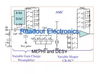
ASIC 1:Source Synchronous Double Data Rate Transceiver 4 optical link each at 622Mbp/s Features: transmitter receiver • Source synchronous design; clock is sent along with data over the optical channels • No-PLL based clock recovery circuits are needed. • Efficient channel use by Double Data Rate(DDR) • Scalable to multiple channels • Adjustable transmitter power and receiver gain • Fully tested at 0.6Gbps per channel • Data rate limited by CMOS I/O VCSEL driver Photo Detect 8:1 serializer 1:8 deserializer Din(7:0) data1 Dout(7:0) clock1 Din(15:8) clock2 Dout(15:8) 8:1 serializer 1:8 deserializer data2 ClkIn (78MHz) ClkOut (78MHz) clk4x (311MHz) (b) chip architecture Transmitter digital circuits 1*4 PD array & receiver ckt Receiver digital circuits 1*4 VCSEL array & driver circuit. (a) Chip microphotography
Ch 1 Ch 1 Ch 2 Ch 2 Ch 3 Ch 3 Ch 4 Ch 4 ASIC2: Parallel Optical Links with instant power-up/down capability CML IN Driver ckt. & VCSELs PD & Receiver CMLOUT Drv Drv Drv Drv TX Power on RX Power on • Channel is able to power-down/up within 3 nanoseconds • Individual power-down control for every channel • adjustable bias and modulation current controlled by on-chip digital registers • Data rate at 2.5Gbps
System Integration Back view of the CMOS chip with VCSEL front view of theCMOS chip with PIN 4 x 1 RX IC Hybrid COB Free-space optical Link GHz bypass connectors 4 x1 TX IC Hybrid COB FR4 mother- board Xilinx FGPA controller Gigabit test-bed
Measurement Results 2-Gb/s 2.5-Gb/s 3-Gb/s
Instant On/off optical link demonstration PWR_ON_SIGNAL 500ps PWR_OFF_SIGNAL • 2-Gbps VCSEL power-on/off eye • 2-Gbps link (tx+rx) power-on/off eye
(a) Normal operation (b) At worst case scenario Link Performance for Continuous Operation Eye diagrams: Link eye diagram measured after 11 hours of operation @ 2-Gbps BER measurement: No errors after running for 11 hours continuously. Bit Error Rate < 1E-14
Free fabrication and flip-chip bonding service Sponsored by OIDA/PTAP program Two types of Driver circuits designed VCSEL driver circuit GSE driver circuit Recent Design submission using 0.25um Technology • GDS submitted on 02/08/05 • Non-gold bumped die shipped on 05/31/05 • Gold bumped die shipped on 06/20/05 • Flip-chip bonded OE devices shipped on 07/15/05
160ps 60ps Simulation Results • GSE driver • 6.25-Gbps/channel • Bias: up to 40mA • Modulation current: 40 mA • VCSEL driver • 15-Gb/s/channel • Bias: ~ 1mA • Modulation:~ 5mA • Data rate can be pushed higher by using • inductors peaking
Proposed Single-chip Approach--integrating SerDes, Transceiver and OE Devices 10G Transceiver Module • Improve performance • No off-chip high speed lines • Flip-chip bonding reduce capacitance and inductance • Reduce power consumption • No 50-Ohm transmission lines between chips Parallel Data Photonic RX De- seriliazer Decoder Optical data TIA/LA RXREGclock PIN Clock/Data recovery clock is embedded in the serial data stream Flip-chip bonding PLL REFclock VCSEL seriliazer encoder Parallel Data Driver TX
Support from Peregrine • Peregrine is highly interested in collaboration • We have access to their advanced fabrication technology • $30k for 3mmx3mm MPR • $15k for Flip-chip bonding service • Technical Support