Download
1 / 64
640 likes | 854 Views
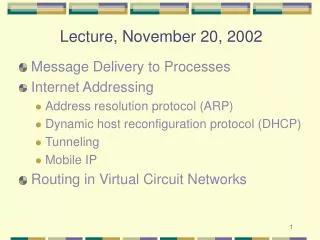
Status of ADF System Design November 2002. D. Calvet DSM/DAPNIA/SEDI, CEA Saclay 91191 Gif-sur-Yvette Cedex. Content. Algorithm and Simulation Analog Splitters ADF board ADF crate Timing card Test bench Software Summary. ADF System. 1280 cables (differential analog data) from BLSs.

E N D
Status of ADF System DesignNovember 2002 D. Calvet DSM/DAPNIA/SEDI, CEA Saclay 91191 Gif-sur-Yvette Cedex
Content • Algorithm and Simulation • Analog Splitters • ADF board • ADF crate • Timing card • Test bench • Software • Summary 2
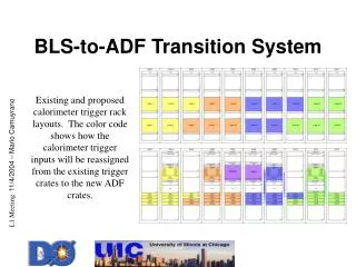
ADF System 1280 cables (differential analog data) from BLSs Timing Crate 0 ADF 0-19 V M E Crate 1 ADF 20-39 V M E Crate 2 ADF 40-59 V M E Crate 3 ADF 60-79 V M E Timing 60 x 2 Gbit/s 60 x 2 Gbit/s TAB 0-7 GAB C P U SCL V M E V M E V M E V M E V M E 60 x 2 Gbit/s 60 x 2 Gbit/s SCL Trigger Control Computer L1 framework, L2/DAQ • 32 analog channels + 3 (ou 1?) output 2 Gbit/s per ADF board • 20 ADF boards+ 1 interface per crate (« VME Interconnect ») • 80 ADF boards in 4 VME crates in total • 1 board for timing distribution 3
Trigger Pickoff Signal 396 ns Measured on one EM channel 132 ns • Rise time too long for operation at 132 ns: • Let E=energy deposited for BC #N: 75% of E observed at BC #N-1: can cause fake trigger at BC #N-1 that causes a veto for BC #N which is lost! • Long tail: 80% of max after 132 ns; 20% after 396 ns • -> Digital Signal Processing 4
Algorithm • Algorithm unchanged since Nov. 2001 studies • Close to what is done in other experiments: • ATLAS and CMS: 5 tap FIR @ BC frequency + 3 point peak detector + some logic for saturated pulses • Proposal for D0: up to 8-tap FIR @ BC x 2 frequency + 3 point peak detector -> very conservative wrt rate and number of taps 10 bit 30.28 MHz 10 bit 15.14 MHz 11 bit 15.14 MHz 11 bit 7.57 MHz 8 bit 7.57 MHz ADC 2 8 Tap FIR 3 Point Peak Detector 2 ET Look Up Table Serializer • VHDL coding completed and simulated • 8 channels fitted in FPGA Xilinx Virtex II 500K gates 456 pins 5
Simulation Chain Arbitrary Waveform Generator ADF Prototype Post-proc. Display Analysis, Validation FPGA Eval. kit Hardware Software VHDL Simulation Simulated Energies Trigger Pickoff Measure- ments Filter Generator Filter Sampling Quantization Signal Processing Smooth Decimation Periodization Amplitude scaling, Noise, delay, jitter, pile-up… Anti- aliasing Period T N levels FIR, IIR, other… Floating point, Fixed, precision… • Largest part of software operational • Some improvements to make; work on coherence with VHDL simulation results 6
Analog Signal Splitter Card • Active board for duplicating differential analog signals from 8 trigger towers • Collecting raw data samples • Test ofADF board prototype in parasitic mode Trigger L1 calorimeter Run IIa (in operation ) CTFE CTFE CTFE Analog Signal Splitter Card Prototype ADF Cables from BLS 7
Analog Splitter • One board cabled • Minor error found: • DC/DC converter need to be soldered on other side of PCB due to top/bottom view inversion • Missing thermal drain below operational amplifiers • -> Corrected PCB not mandatory but will be done • Test bench • - quickly made differential source (AD829), cables and adapted loads • Preliminary tests (sinus input) • Connector pinout is correct, all channels work; gain is correct • Bandwidth: over 10 MHz • More tests needed • - arbitrary waveform generator • Schedule for installation in D0? 8
ADF Board Status • Core FPGA (digital filter) • VHDL coding 100% completed and simulated • 8 channels synthetized, fitted in XC2V500 FG456 -4 • Post-route simulation done • VME interface and bootstrap interface • VHDL coding 100% completed and simulated • Programmable logic fitted in XC9572XL –10 TQ100C CPLD • Board-level VHDL simulation • Includes 4 FPGA’s + VME interface + bootstrap logic • Started for behavioral model • Some control software was developped to exercice the VHDL model -> Several errors in the FPGA logic were found and are being corrected • Schematic capture: will start in November 2002, although board level simulations not 100% completed - Aim for PCB designed ~end January 2003 9
ADF board Block Diagram VME Bus (J1) Backplane (J1 reserved pins) SCL interface cable (J0) Idem #2 Idem #3 VME interface 8 80 8 80 Channel Link serializer 36 FPGA #1 Channel(8-15) FPGA #0 Channel(0-7) Config. SPROM 4 Parity #1, #2, #3 CLK Channel Link serializer (J0) 64 MHz 36 24 JTAG FPGA Programmation Interface 32 Channel data Channel Link serializer 36 FPGA #2 Channel(16-23) FPGA #3 Channel(24-31) 5 V 3.3 V Parity BX count Start of frame Frame 8-10 bit 1.5 V 8 80 8 80 1 3 1 3 ADCs ADCs 3.3 V Z DAC ADC drivers Z DAC ADC drivers -5 V 8 analog input (J2) 8 analog input (J2) 10
ADF Channel Analog Section • Design in progress…: • Digitization with 10-bit precision, identical input range for all channels • Passive RC filter for anti-aliasing; Octal DAC MAX5307 for zero adjust 11
ADF Channel Digital Section Channel #N • Logic duplicated for each channel + common logic for channels within the same FPGA History buffer History buffer 10-bit serializer S E L E C T Input Selector Input Decimator Convolver Peak detector Et LUT 8-bit serializer out ADC #N Magnitude comparator LFSR delay Self trigger History buffer constant ADC clock Configuration registers Bus interface Shared signals Address, RD/WR* Data In, Data Out Common logic 12
Input Decimator and ADC Clock BC • ADC Clock: • Copy or inverted copy of internal 30.28 MHz clock made with DDR reg. • Input decimator • Keep 2 samples per BC out of the 4 converted depending on phase selection • 4 possible phase value: phase adjustment 1:8 BC i.e. 16.5 ns • Samples output on 2 parallel stream to interface to dual-branch convolver • Decimation done with constant latency wrt BC clock 30.28 MHz Channel #N 0° 180° Phase selection (0) BC clk (a) ADC clk CLK CLK* D ADC CLK (a) ADC out 0 1 2 3 DDR register (a) odd/even 30.28 MHz Even samples 0 2 10 Input Decimator (a’) odd/even 1 3 Input samples 10 7.57 Msps Odd samples (b) ADC clk 10 30.28 Msps CE CLK PH (b) ADC out 7.57 Msps 0 1 2 3 (b) odd/even Enable 2 0 2 (b’) odd/even 60.56 MHz Phase selection 1 3 13
Input Decimator and ADC Clock • E.g. Phase Selection=0; BC period = 128 ns: • Samples 0, 4, 8, 12, 16 … are selected • Samples 0, 8, 16… on q_even with latency of 0.5 BC wrt rising edge of clk_bc • Samples 4, 12, 20… on q_odd with latency of 0.5 BC wrt rising edge of clk_bc 14
Convolver Channel #N Selector 8 tap Shift reg. 18 x 18 bit unsigned multiplier Even samples 10 X 16 Adder XY 7.57 Msps Coef. bus 8 x 6 bit DPSRAM Accumulator 19 Y 17 Out Selector 8 tap Shift reg. 18 x 18 bit unsigned multiplier Even samples 10 X 15.14 Msps 16 XY 7.57 Msps Coef. bus 8 x 6 bit DPSRAM Y Convolver out ready Bus interface 60.52 MHz Shared Control Logic Address, Data in Data out • Dual-branch convolver: • faster : 8 tap @ 15.14 MHz (Single branch: ~4-5 tap) • But more work because no IP core. Anyway if Xilinx Coregen IP core: no generic size in VHDL code, control logic not shareable 15
Peak Detector Output Decimator Channel #N MSB 16 D D Decimator :2 16 Output From convolver 19 Q Q « 0 » 7.57 Msps 15.14 Msps 3 Load Peak Detector Off A A>B & B A A>B Decimate selection B 60.52 MHz Shared Control Logic Output ready • 3-point peak detector followed by :2 decimator • Only 16 MSB of convolver output compared to save logic • Peak detector On/Off control • Keep 1 output out of 2 (2 possibilities) with constant latency 16
Peak Detector Post Divisor Channel #N MSB K Overflow OR From peak detector 16 MSB 10 10 Output 7.57 Msps 16-K In 7.57 Msps LSB LSB 2 Post divisor 1, 2, 4 or 8 • Arithmetic right shift for result scaling • Programmable post divisor value: 1, 2, 4 or 8 • MSB’s that are lost are OR’ed together to make overflow bit • Stage in combinatorial logic 17
Et Look Up Table Channel #N 2K x 8 bit DPSRAM ‘0’ A_WR Overflow A_A10 Calibrated Et output A_D7 A_D0 8 7.57 Msps Scaled Peak 10 A_A9 A_A0 7.57 Msps B_CS 60.52 MHz A_CLK B_WR B_A10-0 B_D7-0 13 8 D in/out Bus interface Address, Data in Data out • Look up table for final Et result • Conversion from 10 bit to 8 bit Et • Arbitrary conversion function (e.g. implement clipping, saturation) • Programmable output value when arithmetic overflow (uses ½ LUT) 18
Serializer and Latency Adjust ADC raw data (history) 10 Channel #N S e l e c t IN 9-0 Q0 Constant 8 S e l e c t Parallel load Shift Register Programmable Length shift register Serial Out ADC raw data 8 60.52 Mbps 8 7.57 Msps 1..32 IN 7-0 Q0 In Out Et 8 2 3 LFSR 8 2 coarse Latency Adjust Serializer source 60.52 MHz fine Send raw Bus interface Address, Data in Data out • 4 possible sources of data for 8-bit serial stream • 8 MSB of ADC value, Et result, Constant value, pseudo-random value • Switch to 10-bit frames when sending raw ADC samples • Per channel coarse latency adjust (+0 to +3 BC); common fine adjust (+1/8 BC to +7/8 BC) 19
LFSR Channel #N 16-bit Parallel load Shift Register XNOR SIN Q15 Q14 Q13 Q12 Q11 Q10 Q9 Q8 Q7 Q6 Q5 Q4 Q3 Q2 Q1 Q0 LFSR Out 8 16 Parallel In 15-0 60.52 MHz Shift Enable Bus interface Address, Data in Data out • 16-bit pseudo-random generator • Per channel programmable seed • 8 LSB’s can be sent to ADF output serial stream • Common shift enable for inter-channel synchronization 20
History Buffer Channel #N ADC input 10 10 Shift R. Input Selector DIN_A DPRAM 1024 x 18 bit Selector Et result 8 ADDR_A Input decimator Out odd Out even WR_A DOUT_A « 00 » CE_A WCLK_A Convolver output 16 Test mode Phase selection CLK BCx8 T Phase sel.(0) DIN_B Pr. ADDR_B CE WR_B DOUT_B CE_B Shared Logic WCLK_B Bus interface Address , Data in Data out • History buffer used for test mode without ADC input: • Play at input of digital filter digital values pre-loaded via bus interface 21
History Buffer Usage Convolver Out(K-L) 0x000 Et(K-L) Raw ADC(K) 0x001 Memory content shown for for phase selection = 0 or 2 For phase selection = 1 or 3, the content of odd and even addresses is exchanged Convolver Out(K-L) 0x002 Et(K-L) Raw ADC(K+1/4) 0x003 BC #K Convolver Out(K-L+1/2) 0x004 Et(K-L) Raw ADC(K+1/2) 0x005 Convolver Out(K-L+1/2) 0x006 Et(K-L) Raw ADC(K+3/4) 0x007 Convolver Out(K-L+1) 0x006 BC #K+1 Et(K-L+1) Raw ADC(K+1) 0x007 0x2FF • Shared 1024 x 18 bit SRAM written at BC x 8 • 512 x 10 bit: raw ADC sample (sample change at BC x 4) • 256 (x 2) x 16 bit: convolver output (result change at BC x 2) • 128 (x4) x 8 bit: Et filtered output (result change at BC x 1) 22
State Machine for raw sample RAM Reset FPGA #0, #1, #2, #3 Frozen Freeze after send Resume command Resuming Resume after send Send count not reached Sending Resume complete Do not send raw ADC data Send raw ADC data Suspending Recording L1 accept, L1 monitoring, L1 self, L1 software Resume after send: if L1 accept and none of L1 monitoring, L1 self, L1 software flags Freeze after send: if any of L1 monitoring, L1 self or L1 software flags L1 accept, monitoring, self, software are previously ANDed with corresponding mask flag 23
BX and Turn Count Serializer ’00’ FPGA #0, #1, #2, #3 8 30-bit // load Shift register Init Req Geo. section 16-bit up counter Reset 16 Q ’00’ 30 Clk Programmable Length shift register 8 BX Marker ’00’ Serial BX/TC Preset ‘1’ 1-159 up counter =159 1..32 Q0 In Out 8 Q 7.57 MHz 60.52 Mbps Load 2 3 Clk coarse Latency Adjust 60.52 MHz fine • When sending 8-bit frames to TAB: • Load activated every 8 ticks: serial stream is 8-bit current BX count • When sending 10-bit frames to TAB: • Single shot on load: serial stream is: BX count, 8 LSB of turn count, 8 MSB of turn count; these 3 bytes are put in 10-bit frames (pad: 00) 24
Last L1 BX and Turn Count FPGA #0, #1, #2, #3 Reset 16 Turn Count 16 Last L1Turn Count D Q Single shot after Suspending Clk Resuming recording Reset 8 8 Last L1 BX Count BX Count D Q Clk Bus interface Address , Data in Data out • After trigger causing raw sample recording to freeze: • Latch current BX and Turn count • Made available for read via bus interface • Reset occurs when raw sample recording resumes 25
Parity Generation Parity output for FPGA #1, #2, #3 Xor 8 Channel serial data FPGA #0 only Xor Parity out BX/TC serial data Frame_8_10 Frame Parity out #1 Parity output for FPGA #0 Parity out #2 Parity out #3 • Parity of 8 channel data calculated by FPGA #0, #1, #2, #3 • Partial parity of FPGA #1, #2, #3 sent to FPGA #0 • FPGA #0 computes global parity over 32 channels and ctrl signals • Global parity sent to TAB over Channel Link 26
Start Of Frame • Frame active when LSB of data is present on serial stream 27
Frame_8_10 • Frame_8_10 low when sending 8 bit frames; high when sending 10 bit frames (sending raw ADC data following L1 Accept) 28
ADF Latency (partial) • 6.65 BC from peak at ADC digital output to last bit of result out of FPGA 29
Channel Link Interface FPGA #0 DC Balance Driving logic to be defined DS_OPT CLK DDR 60.52 MHz Parity BX/TC Frame_8_10 Start Of Frame 8 Channel serial data (32+4) x 60.52 Mbps = 2.17872 Gbps 8 FPGA #1 Channel serial data 8 FPGA #2 Channel serial data 8 FPGA #3 Channel serial data • 36 bit lanes used (out of 48 available): • - 8 channel data from by FPGA #0, #1, #2 and #3; 4 control lanes • Clock + DC balance control bit + option bit 30
VME interface and bootstrap logic PROG_B0..3 XC17S05 SPROM Slot ID 5-0 JTAG C_CS_B0..3 Digital Filter FPGA’s AM XC9572 CPLD C_RD_WR* CY7C960A VME Slave Interface DS1*-DS0* C_CLK AS* INIT_B DTACK* DONE A23-A16 WRITE* BUSY VME BUS CS0*-CS3* 74 LVC 373 A23-A1 A15-A2 LACK* D15-D8 DBE3-DBE0 74 ABT 543 74 LVC 245 D15-D0 D15-D0 WR/RD* • Download FPGA configuration via VME: • - all 4 FPGA’s loaded at once or different config on each FPGA • VME interface A24 D16-D8 only; no DMA; no interrupt • Provides 5V <-> 3.3V conversion; Virtex 2 I/O not 5V tolerant 31
Types of L1 Trigger for ADF System • D0 Framework L1 Accept • Generated by D0 framework; sent to all Geographic Sections via SCL • Fanout to ADF system by SCL Interface Fanout card (SCLIF) • Indicates that current BC is a L1 accepted event • L1 Accept with Monitoring • Generated asynchronously by TCC to indicate that monitoring data of Geo section should be kept for one of next D0 framework L1 Accept • Sent synchronously by D0 L1 framework to Geo section by L1 Qualifier • If L1 Framework accept and L1 Qualifier for Monitoring asserted: the current L1 is to be monitored; all history data kept for TCC readout • L1 accept with monitoring flags are fanout to ADF system by SCL Interface Fanout Card 32
Types of L1 Trigger for ADF System • L1 Software Accept • Generated asynchronously by TCC to indicate that one of the next L1 crossing should be treated as D0 Framework L1 Accept by ADF system • Issued by one ADF card upon asynchronous write by TCC, • bounced-back synchronously to ADF system by SCLIF card • L1 Self trigger Accept • Generated by each ADF channel when ADC input greater than programmable threshold • Wired-Ored for all channels on an ADF card • Wired-Ored for all ADF cards within each ADF crate and sent to SCLIF • OR-ed by SCLIF and sent back to all ADF cards synchronously 33
Actions upon L1 Trigger for ADF • D0 Framework L1 Accept • Send burst of raw ADC data to TAB (if feature enabled); no action if disabled • -> TABs get raw ADC samples around BC that caused L1 trigger in D0 • L1 Monitoring accept • Send burst of raw ADC data to TAB (if enabled) then freeze history buffer in all channels • Wait resume recording command to start saving data in history buffer • -> TCC can read ADC raw samples and intermediate results for some BC’s that caused L1 trigger in D0 • L1 Software accept • Same action as L1 monitoring accept • -> TCC can read ADC raw samples and intermediate results for random BC’s that did not cause a L1 trigger in D0 (used to check correct operation of ADF system) • L1 Self trigger accept • Same action as L1 monitoring accept • -> TCC can record the shape of pickoff pulses on each channel to determine (off-line) optimal digital processing parameter sets 34
Limitations • History buffer common for sending raw ADC samples to TAB and for read-out via TCC • When recording is frozen (i.e. TCC read-out in progress), sub-sequent L1 accept will not trigger sending of raw ADC samples to TAB • -> Raw ADC samples for these L1 accept are lost (but digital filter output continues to flow) • If no L1 Monitoring or L1 software accept are issued, raw sample recording is never frozen, raw samples for all L1 accept can be sent to TAB • Links to send filtered data and raw ADC data to TAB are the same • While sending out raw ADC data to TABs, flow of filtered data is stopped -> can introduce dead-time for L1 if sending time is larger than that of other sub-systems • -> e.g. sending raw samples of 8 BC around L1: 320 bit / channelsending time = 5.28 us 35
SCL signals fanout • 1 cable to one ADF board in each ADF crate • ADF board where cable is plugged in charge of fanout within crate A D F # 1 A D F # 10 A D F # 20 A D F # 1 A D F # 10 A D F # 20 SCL Receiver Mezzanine SCL Crate #0 Crate #1 SCL Interface Fanout Card (SCLIF) 8 pairs Crate #2 Crate #3 1-2 spare A D F # 1 A D F # 10 A D F # 20 A D F # 1 A D F # 10 A D F # 20 5-6 cables ~3 m; 2 mm HM connector 8 pairs; LVDS ADF board for intra-crate fanout 36
SCL Interface and Fanout card • VHDL design in progress • 3U or 6U mechanics; No slow control • No slot available in ADF crate -> back of slot 0 if enough space J1 J2 PROM configuration SCL Receiver Mezzanine (FNAL) FPGA logic HM 2 mm connector 4-6 Cables to ADF crate SCL Fiber/Cable • Baseline: segmentation 0.2 x 0.2 37
SCLIF to ADF communication • SCLIF to ADF cable pinout (preliminary) Cable detect rem,loc - GND - BC Clock CMDD (SCLIF->ADF) - GND - CMDU (ADF->SCLIF) BUSY (ADF->SCLIF) - GND - Self Trigger (ADF->SCLIF) ERROR (ADF->SCLIF) - GND - SPARE Cable detect remote: wired to GND on SCLIF card; pullup resistor on ADF card Cable present local: pullup resistor on SCLIF card; active low output of ADF logic • CMDD: Command Downstream (SCLIF to ADF system) 8 bit per BC (60.56 Mbit/s link) 7 6 5 4 3 2 1 0 Geographic Section Init Request Resume ADC raw sample recording Sofware L1 Accept Self generated L1 Accept L1 Accept for Monitoring D0 Framework L1 Accept BX Marker Unused 38
SCL to ADF communication (con’t) • CMDU: Command Upstream (ADF to SCLIF system) 8 bit per BC (60.56 Mbit/s link) 7 6 5 4 3 2 1 0 Geographic Section Init Acknowledge Resume ADC raw sample recording Sofware L1 Accept Unused • Bits « Resume ADC raw sample recording » and « Sofware L1 Accept »: • - Issued by one ADF card upon Write action by TCC to appropriate register • Bounced-back by SCLIF to all ADF crates and cards • -> Equal-delay path from TCC to all ADF cards • Bit « Self L1 Accept »: • Wired-OR self trigger signal for all ADF card within the same crate • Per crate Self Trigger signal send on cable wires to SCLIF • All per crate self trigger signals OR-ed by SCLIF to make Self Trigger bit • Self trigger bit sent to all ADF simultaneously in CMDD serial stream 39
Intra ADF crate Signal Distribution RJ0/J0 Remote cable present ADF Board #N (FPGA #0) Local cable present ERROR_BUS_OUT (FPGA #0, #1, #2, #3) CLK BC SCLIF Cable (to one ADF board per crate) (FPGA #0, #1, #2, #3) Self trigger BUS_OUT CMDD (FPGA #0, #1, #2, #3) Serial to // BUSY_BUS_OUT CMDU BUSY Self Trigger ERROR CLK_BC_BUS_OUT CMDD_IN(7..0) CLK_BC_IN P1 VME 64 P1 (reserved) bussed lines CMDD(7..0)_BUS_OUT BUSY_BUS_IN ERROR_BUS_IN Self trigger BUS_IN CMDD(7..0)_BUS_IN (373) CMDD(7..0)_BOARD_OUT (CDCV304) CLK_BC_BUS_IN CLK_BC_BOARD_OUT • ADF board where SCLIF cable plugged: makes fanout of signals on backplane; other ADF boards tri-states outputs to bus • All ADF boards get signals from backplane; local fanout for 4 FPGA’s 40
FPGA Internal Clock Generation Digital Clock Manager #1 CLK_FB CLK FX 30.28 MHz , phase = 0° CLK_IN CLK FX_180 30.28 MHz , phase = 180° 7.57 MHz On board Fanout chip Digital Clock Manager #2 CLK_FB CLK FX 60.56 MHz , phase = 0° CLK_IN CLK FX_180 60.56 MHz , phase = 180° FPGA #0, #1, #2, #3 • On-chip BC clock multiplication by 4 and 8 • All logic driven at BC x 8 = 60.56 MHz • ADC clock from clock at BC x 4 = 30.28 MHz 42
System wide BC Clock phase align earliest tower ~70 ns latest tower Back- plane bus ADF #20 SCL Mezz. CLK_BC 7.57 MHz clk clk 1 cable 9 Analog ADC input 5 clk clk 2 6 Programmable delay line BC clock at FPGA 7 8 3 ADF #1 FPGA 4 SCLIF ADF Crate • Clock distribution: expected delay dispersion: ~3 ns; jitter: 400 ps? • Programmable delay line on SCLIF clock: adjusted so that all analog peaks at ADC input fall within same BC period 43
ADF Crate • Crate to be delivered ~November 2002 • Custom backplane: design not started 20 ADF boards VME Interface VME64 backplane Custom backplane ADF Board (6U) J1 1timing cable J0 60 (20?) TABs cables J2 320 BLSs cables Fan unit Power Supply Rear-side Right view 44
Custom Backplane • Passive backplane; controlled impedance traces • Need some mechanics to hold (heavy) cables External Side: 20 x 16 AMP 8 points connectors option with J0 transition connector Internal Side: 20 VME 160 points connectors 45
RJ0 Usage (preliminary) 1 2 3 4 5 6 7 8 9 0 1 2 3 4 5 6 7 8 9 1 2 3 4 5 Signal + Signal - GND Signal + Signal - TAB Link #1 TAB Link #2 TAB Link #3 SCLIF Cable • 19 x 5 2 mm Hard Metric connector can accomodate: • 3 cables to TAB each 8 or 10 pairs (if 8-pair cable: GND 5 pins between each cable) • 1 cable to SCLIF (for one ADF card in each crate) • Cable to TAB • 8-pair cable could be 7 signals + 1 clock : transmit 7x6=42 bit of Channel Link (out of 48), altough 36 bits are assigned at this stage • Cable detection feature? 46
Power Estimation • Logic 3.3 V • 0.75 A per board -> converted from +5V with DC/DC @85% eff.: 0.6 A / board 12 A /crate • FPGA Core 1.5V • 3.2 A per ADF board • -> converted from +5V with DC/DC @85% eff.: 1.2 A / board 23 A /crate • ADC 3.3 V • 2.8 A per board; 60 A per crate • ADC driver –5 V • 0.6 A per board; 12 A per crate • Crate requirement: +5V 45A; +3.3V 60A; -5V 12A 47
16 R R’ 4R 8R 2R R ADF Power circuitry • FPGA Core 1.5V • converted from +5V with DC/DC converter EL7564 • Per slot startup delay to power each board after the other • Logic 3.3 V • converted from +5V with DC/DC converter EL7564 +5V Soft Start C Geographic address pins 0V • ADC 3.3 V • - taken from VME 64 P1 connector • ADC driver –5 V • taken from VME 64 P1 connector 48
Test bench ADF board • Standards items + dedicated mezzanine card(s) -> Channel Link de-serializer mezzanine: redundent with Nevis development -> Mezzanine with 1 ADC (to test 1 analog input + digital filter) PCI/VME Interface Waveform generator G Evaluation kit FPGA Virtex 2 Deserializer A D F V M E Digital I/O Card High Speed cable VME crate PC Dedicated Mezzanine card 50