Permalloy square dots
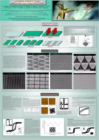
PATTERNED MAGNETIC FILMS: FABRICATION AND CHARACTERIZATION. Lithographic process.

Permalloy square dots
E N D
Presentation Transcript
PATTERNED MAGNETIC FILMS: FABRICATION AND CHARACTERIZATION. Lithographic process By means of Electron Beam Lithography (EBL) and X-Ray Lithography (XRL) it is possible to prepare arrays of magnetic structures with different materials and geometries. The steps of the process are illustrated in the figure (beside): a magnetic continuous film is coated with a resist layer and then exposed by an electron or X-ray beam; the exposed resist areas are then removed by an appropriate solution (developer) and the underneath film by an etching process; finally the residual resist is simply removed by a hot acetone wash. In the EBL technique a focused electron beam directly writes the desired pattern on the resist (fig. a, below), simply moving the beam’s spot on the sample. Instead, in the XRL technique the exposed areas are selected by a mask between the X-ray source and the sample (fig. b). Hence, EBL is a direct writing technique and allows to change easily the desired pattern, whereas XRL is a parallel writing technique that is faster than EBL and allows to produce large patterned areas; moreover X-rays’ great penetration depth permits the patterning of thick resist layers and films. So the combined use of EBL and XRL is a powerful tool in the fabrication of micro- and nano-structures with different geometries and thickness, spreading over large areas. Resist layer Continuous magnetic film Silicon substrate Magnetic film Resist coating Exposure Resist Development Film Etching Final result b) Schematic arrangement for XRL. a) Schematic apparatus for EBL. Magnetic measurements Manufactured samples In this work we use Electron Beam Lithography (EBL) and X-Ray Lithography (XRL) to prepare arrays of magnetic structures: in particular, Permalloy (Fe20Ni80) square dots and triangular antidots (fig. 1, 2) as well as X-ray masks (fig. 3, 4) are fabricated by means of EBL technique, while the masks are used to pattern a Nickel film and a Co-Au multilayer (fig. 5, 6, 7) by means of XRL technique. The combined use of EBL and XRL allow us to pattern thick film with a good lateral resolution: dot dimensions range from 2m to 250nm and spacings between the dots from 4m to 100nm, while their thickness range from 100Å to 350Å; all the patterned areas are (11)mm2. A negative (SAL601) chemically amplified resist is used for the e-beam lithography of the square and triangular patterns; then the structures are transferred onto the Permalloy film by an argon ion milling process. Silicon nitride (Si3N4) membranes 100nm thick deposited on a Si wafer 300m thick and coated with a base plating of Cr-Au are employed for the fabrication of the x-ray masks: a positive (UV III) chemically amplified resist is used and the resist pattern is exploited to perform an electrolythic growth of 350nm thick gold, in order to obtain a successful mask effect to X-ray radiation. X-ray lithography is performed with a thick (800nm) SAL601 resist layer and the pattern is transferred onto the Ni film and the Co-Au multilayer by an argon RIE process. Fig. 1, 2: Permalloy triangular shaped antidots by means of EBL. The magnetic film is 10nm thick, the triangles are equilateral with 1m side and 100nm spacing between the antidots. Fig. 3, 4: X-Ray masks by means of EBL. The gold-structures (350nm thick) are grown by electrolysis Fig. 5, 6, 7: Nickel patterns of dots by means of XRL. The Ni film is 35nm thick, dots dimensions range from 1m to 250nm whereas spacings are 250nm and 100nm. Permalloy square dots Three different patterns of permalloy square dots are manufactured: the dots have 2m side and spacing of 1, 2 and 4m. Beside there are some MFM images (dot side 2m, spacing 2m) at increasing values of the external field H. It is evident the approach to the saturation, where all the dots show a uniform magnetization M (fig. c). In fig. a we have the zero-field situation: many dots present a four-domain configuration (shown in fig. d), which is the expected configuration for an isolated dot; however there are also different configuration. Investigating the presence of four-domain dots in the three different patterns (in the zero-field condition) it is put in evidence a weak inter-dots dipolar coupling: in fact the number of four-domain dots increases with increasing spacing between the dots (table below). L.I.LIT. Laboratory for Interdisciplinary LIThography P. Candeloro1, A. Gerardino2, L. Vaccari1, M. Altissimo1, S. Cabrini3, L. Businaro1, D. Cojoc1,4, M. Prasciolu1, F. Feri1, F. Romanato1, G. Carlotti5, G. Gubbiotti5 and E. Di Fabrizio1 1 LILIT-NNL (National Nanotechnology Laboratory) , TASC-INFM Nanolithography beamline at Elettra Synchrotron Light Source, Area Science Park, S.S.14 km 163.5, 34012 Basovizza, Trieste, Italy 2 CNR-IESS, Istituto di Elettronica dello Stato Solido, Via Cineto Romano 42, 00156 Roma, Italy 3 Elettra Synchrotron Light Source, Area Science Park, S.S.14 km 163.5, 34012 Basovizza, Trieste, Italy 4 TEF Dept, Univ. ‘Politechnica’ of Bucharest, Romania 5 INFM, Dipartimento di Fisica, Università di Perugia, via A. Pascoli, 06100 Perugia, Italy Contacts: difabrizio@tasc.infm.it, patrizio.candeloro@elettra.trieste.it Summary of the measurements The magnetic properties of the samples are investigated by Magnetic Force Microscopy (MFM), Brillouin Light Scattering (BLS) and Magneto-Optical Kerr Effect (MOKE). In some cases (Permalloy square dots) MFM measurements show clearly the domain configuration and their evolution during a hysteresis loop, putting in evidence a weak inter-dots dipolar coupling; moreover the BLS measurements reveal the quantization of the Damon-Eshbach spin-wave mode. By means of BLS, in all the other cases, we obtain the demagnetizing factor of the structures and we find a good agreement with the expected theoretical values [1, 2]. Finally, in each case, comparing MOKE measurements of the continuous film with the patterned ones, put in evidence strong effects due to the lateral confinment: in the Nickel dots the magnetic anisotropy of the film is totally modified by the shape anisotropy, so much that the easy direction in the continuous film becomes the hard one in the patterned film. [1] A. Aharoni, J. Appl. Phys.83, 3432 (1998) [2] A. Aharoni et al., J. Appl. Phys.87, 6564 (2000) The dispersion of the DE mode was measured by varying the angle of incidence light in BLS, both for the continuous film and for the pattern 2m spacing. Due to the presence of demagnetizing fields inside the dots, the dispersion curve of the pattern is lower than that of the continuous film, according with the following spin-wave formula: where is the gyromagnetic ratio, Hi is the internal field, A is an exchange costant, MS is the saturated magnetization, q|| is the transferred wavevector (q||=2kisin , with incidence angle) and d is the thickness of the magnetic film. With the same external field H0 we have different Hi in the two cases: Hi = H0 continuous film Hi =H0 – 4pDMS patterned film where D is the demagnetizing factor. A quantitative analysis of the two curves allows to esimate the value of the factor D. The figure above shows a comparison between a BLS spectrum of the pattern with dots’ spacing 2m and the corresponding spectrum of the continuous permalloy film; it is evident that the superficial spin-wave mode (Damon-Eshbach mode, DE) is quantized in the case of the dots. Obviously this is due to the lateral confinment imposed by the dots’ edges. Permalloy triangular antidots In the figure on the left the hysteresis loops (MOKE measurements) of the triangular antidots and of the continuous film (in the inset) are reported. The loops are measured in the MOKE longitudinal configuration, with the external field applied parallel to the sample surface. The loop of the continuous film is highly rectangular and has a coercive field of less than 10 Oe. Instead, the loops of the patterned film have a gradual approach to the saturation and a coercive field much increased. The former effect is due to the demagnetizing field associated with the magnetic poles at the edges of the antidots, whereas the increasing of the coercive field is connected to the fact that the triangular holes act as pinning centers for the magnetization reversal. As shown in the figure, the coercive field HC is not the same in different in-plane directions. In the figure on the right, the behaviour of HC as a function of the in-plane applied field is reported: it obviously has the perodicity of the pattern and shows maxima at 0°, 60° and 120° and minima at 30°, 90° and 150°. The directions where the coercivity is maximum correspond to the directions where continuous stripes are recognized. These directions are easy axis of magnetization and it is more difficult to reverse the magnetization. Nickel rectangular dots In contrast with permalloy, nickel exhibits magnetic anisotropy also in the case of a continuous film. Below, the figure on the left shows the hysteresis loops for the continuous Ni film, at 0°, 33° and 90°; the differences in the three loops are due to the magnetic crystalline anisotropy. The largest loop indicates a easy axis of magnetization, whereas the smallest a hard axis. On the rigth there are the loops of the patterned film; the external field is applied in the same directions as in the case of the continuous film (that is 0°, 33° and 90°), where 0° is along one side of the rectangular dots, 90° along the shortest side and 33° corresponds to the diagonal of the dots (inset in the figure). As it is shown the three loops are different yet, but now 90° is a hard axis (smallest loop) in contrast with the situation of the continuous film. This means that the anisotropy due to the presence of the demagnetizing field inside the dots (shape anisotropy) reverses the crystalline anisotropy of the film.