Models
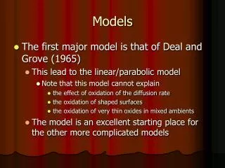
Models. The first major model is that of Deal and Grove (1965) This lead to the linear/parabolic model Note that this model cannot explain the effect of oxidation of the diffusion rate the oxidation of shaped surfaces the oxidation of very thin oxides in mixed ambients

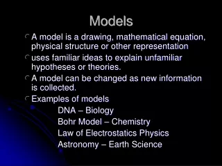
Models
E N D
Presentation Transcript
Models • The first major model is that of Deal and Grove (1965) • This lead to the linear/parabolic model • Note that this model cannot explain • the effect of oxidation of the diffusion rate • the oxidation of shaped surfaces • the oxidation of very thin oxides in mixed ambients • The model is an excellent starting place for the other more complicated models
CHEMICAL REACTIONS • Process for dry oxygen Si + O2 SiO2 • Process for water vapor Si + 2H2O SiO2 + 2H2
OXIDE GROWTH • Si is consumed as oxide grows and oxide expands. The Si surface moves into the wafer. Original surface 54% SiO2 46% Silicon wafer
MODEL OF OXIDATION • Oxygen must reach silicon interface • Simple model assumes O2 diffuses through SiO2 • Assumes no O2 accumulation in SiO2 • Assumes the rate of arrival of H2O or O2 at the oxide surface is so fast that it can be ignored • Reaction rate limited, not diffusion rate limited
Deal-Grove Model of Oxidation • Fick’s First Law of diffusion states that the particle flow per unit area, J (particle flux), is directly proportional to the concentration gradient of the particle. • We assume that oxygen flux passing through the oxide is constant everywhere. • F1 is the flux, CG is the concentration in the gas flow, CS is the concentration at the surface of the wafer, and hG is the mass transfer coefficient
No Silicon dioxide J Silicon N Ni SiO2 Si Xo Distance from surface, x
Deal-Grove Model of Oxidation • Assume the oxidation rate at Si-SiO2 interface is proportional to the O2 concentration: • Growth rate is given by the oxidizing flux divided by the number of molecules, M, of the oxidizing species that are incorporated into a unit volume of the resulting oxide:
Deal-Grove Model of Oxidation • The boundary condition is • The solution of differential equation is
Deal-Grove Model of Oxidation xox : final oxide thickness xi : initial oxide thickness B/A: linear rate constant B : parabolic rate constant xi: thickness of initial oxide layer t: equivalent time required to grow initial oxide layer
There are two limiting cases: • Very long oxidation times, t >> • xox2 = B t • Oxide growth in this parabolic regime is diffusion controlled. • Very short oxidation times, (t + ) << A2/4B • xox= B/A ( t + ) • Oxide growth in this linear regime is reaction-rate limited.
Temperature (0C) 1200 1100 1000 900 800 700 10.0 1.0 H2O (640 torr) EA = 2.05 eV 0.1 B/A (mm/hr) (111) Si (100) Si 0.01 Dry O2 EA = 2.0 eV 0.001 0.0001 0.6 0.8 0.9 1.0 1.1 0.7 1000/T (K-1) At short times, B/A is the linear rate constantProcess is controlled by the reaction at the Si surface
Temperature (0C) 1200 900 800 1100 1000 1.0 H2O (640 torr) EA=0.78eV 0.1 B(mm2/hr) 0.01 Dry O2 EA=1.23eV 0.001 1.0 0.6 0.7 0.8 0.9 1000/T(K-1) At long times, B is the parabolic rate constant (xO2aB) Process is controlled by diffusion of O through oxide
Deal-Grove Model Predictions • Once B and B/A are determined, we can predict the thickness of the oxide versus time
B P 1200 C Mask thickness (mm) 1200 C 1100 C 1100 C 1000 C 900 C 1000 C 900 C Diffusion time (hr) Oxide as a Diffusion Barrier • Diffusion of As, B, P, and Sb are orders of magnitude less in oxide than in silicon • Oxide is excellent mask for high-temperature diffusion of impurities 10 10 Boron Phosphorus 1 1 0.1 0.1 0.01 0.01 0.1 0.1 1.0 10 100 1.0 10 100
Other Models • A variety of other models have been suggested, primarily to correct the deficiencies of the Deal-Grove model for thin oxides • These include • The Reisman power law model • The Han and Helms model with parallel oxidation paths • The Ghez and van Meulen model to account for the effect of oxygen pressure • Some of these models do a much better job for thin oxides • None are widely accepted
Other Topics • Several topics other than the simple planar growth of wet and dry oxide are important • These include • Thin oxide growth kinetics • Dependence on oxygen pressure • Dependence on crystal orientation • Mixed ambient growth kinetics • 2D growth kinetics
Example: 2D Growth • There are several interesting observations • There is significant retardation of the oxide growth in sharp corners • The retardation is more pronounced for low temperature oxidation than for high temperature oxidation • Interior (concave) corners show a more pronounces retardation that exterior (convex) corners
Example: 2D Growth • Several physical mechanisms are needed to understand these results • Crystal orientation • Oxidant diffusion • Stress due to volume expansion • Kao et al suggested changes to the linear-parabolic (Deal-Grove) model to correct for these effects • Most of these effects are built into the modeling software such as SUPREM IV and ATHENA
Measurement Methods • The parameters of interest include • Thickness • Dielectric constant and strength • Index of refraction • Defect density • There are three classes of measurement • Physical (usually destructive) • Optical (usually nondestructive) • Electrical (usually nondestructive)
Physical Measurements • Simple step height technique (DekTak) • Etch away oxide with HF • Use a small stylus to measure the resulting step height • The resolution is <10 nm • More complex technique uses one or more of the SFM concepts (AFM, MFM, etc) • Technique has atomic resolution • SEM or TEM (electron microscopy) • All require sample preparation that makes the tests destructive and not easy to use in production
Optical Measurements • Most optical techniques use the concept of measuring reflected monochromatic light • If monochromatic light of wavelength shines on a transparent film of thickness x0, some light is reflected directly and some is reflected from the wafer-film interface • For some wavelengths, the light will be in phase and for others it will be out of phase • constructive and destructive interference • Minima and maxima of intensity are observed as is varied
Color Chart http://www.htelabs.com/appnotes/sio2_color_chart_thermal_silicon_dioxide.htm
Optical Measurements • Instrument from Filmetrics(http://www.filmetrics.com)
Optical Measurements • The positions of the minima and maxima are given bym=1,2,3… for maxima and ½,3/2,5/2,… for minima • This is called reflectometry and works well for thicknesses over a few 10’s of nm
Optical Measurements • If one does not know n, or if the film is very thin, then ellipsometry is better • When multiple wavelengths of light are used, the instrument is known as a spectroscopic ellipsometer
Optical Measurements • Here, one uses polarized light. • The measurement may be performed at multiple angles of incidence to obtain a higher degree of accuracy • One can get the index of refraction as a function of wavelength as well as the extinction coefficient • Can be used to measure thickness to <1 nm • Fitting routines are necessary to take into account rough interfaces between Si and SiO2 layers.
Cauchy Equation Sellmeier Equation
Electrical Measurements • These measure properties that correlate directly to the performance of the devices fabricated using the oxides • The dominant techniques is the C—V measurement • The basic structure for the measurement is the MOS capacitor • The usual combination is Si-SiO2-(Al or pSi) • Any conductor-dielectric-semiconductorcan be used
MOS Capacitor + Al tox V Si wafer Al -
http://www.mtmi.vu.lt/pfk/funkc_dariniai/transistor/mos_capacitors.htmhttp://www.mtmi.vu.lt/pfk/funkc_dariniai/transistor/mos_capacitors.htm
C-V Plot http://ece-www.colorado.edu/~bart/book/book/chapter6/ch6_3.htm#fig6_3_5
C-V Plot • Differences between high frequency and low frequency C-V data • Doping concentration in Si near Si-oxide interface • Voltage shift proportional to charged defects within oxide