Lecture 7.1
Lecture 7.1. Device Physics – Transistor Integrated Circuit. Bipolar Transistor Discrete device On Chip Field Effect Transistor (FET) On Chip. Uses Amplify a signal Operational Amplifier Switch On/Off Process and store binary data. Transistor. Switch.

Lecture 7.1
E N D
Presentation Transcript
Lecture 7.1 Device Physics – Transistor Integrated Circuit
Bipolar Transistor Discrete device On Chip Field Effect Transistor (FET) On Chip Uses Amplify a signal Operational Amplifier Switch On/Off Process and store binary data Transistor
Combination of two back-to-back p-n junctions P-N-P or N-P-N Bipolar Transistor
Amplifier Gain • Common-base configuration current gain • =1-(Wb/Lp)2/2 ~ 1 (slightly less than 1.0) • Wb = width of base minus depletion regions • Lp = diffusion length of holes in the base. • Voltage Gain • ce= /(1- ) (values from 400 to 600)
MOSFET Metal oxide semiconductor field effect transistor IGFET Insulated-gate FET NMOS or PMOS MISFET Metal-insulator-semiconductor FET MOST Metal-oxide semiconductor transistor JFET Junction FET FET- (Field Effect Transistor)
MOSFET in Memory Chip Source Gate Drain
Inversion Zone - Poisson’s Eq. • 2U = -/( o ) • Metal on • N Zone P Zone n= - e Nd -p=+ e Na • Boundary Conditions • U=Uo at x=0 • U=0 V at x=
Electron Tunneling • Electron Transmission, T, through thickness, δ. • U=Potential Energy of Barrier • E=Total Energy of Electron
Integrated Circuits • CPU or Memory • First Layer • Transistors • Capacitors • Diode • Resistors • Multi-layer • Wiring • Interconnects • Bonding Pads • Dielectric • Capacitors • Heterostructures
Transistor Switching Speed • PNP vs NPN • N channel is Faster - NPN • Mobility of n (electron is faster than hole)
Much Lower Switching Power • Complementary MOS • N channel connected to P channel • 106 less power for switching • 1 pnp acts as amplifier • 2nd npn does the switching
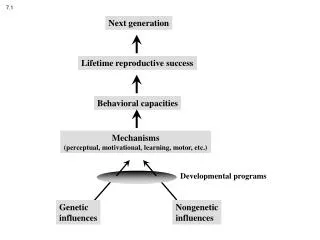
(Gordon E.) Moore’s Law, 1965 Doubling of transistor density every year! Doubling of computer speed in 18 months Doubling of computer size in 18 months Substantial decrease in price with time Price of transistor is 10-6 of original price Integrated Circuit Good for the next 20 years! By 2012 1 Billon Transistors/die 10 Ghz! Limitations by 2017 (gate Thickness) http://developer.intel.com/update/archive/issue2/focus.htm
Size of Transistor $1B/acre 5 layers of Metalization
Scaling Parameter = S >1 • Linear Dimension L1L1/S • Reduce all linear dimenstions by 1/S • Reduce voltage by 1/S • Increase doping Concentrations by S • Decrease time for electron to cross gate • t = L1/Vdriftt/S, Vdrift= eE/me , =relaxation time • Power Dissipated per transistor • P = I V (I/S)(V/S) P/S2
Switching Time Time to take an electron across a gate t = L/Vdrift Vdrift= eE/me , =relaxation time t t/S RC delay time of Interconnects Resistance R= L/A R= L*S/A/S2 RS3 Capacitance C=oA/d C =o(A/S2)/(d/S) C/S RC RCS2 Computer Speed
Copper Wiring/Low K dielectric • Pentium IV • S < 0.18 μm • Clocks @ >2.0 Ghz
DRAM memory Array • Memory Chip • First Layer • Transistors • Multi-layer • Wiring • Interconnects • Bonding Pads • Dielectric • Capacitors • Dielectric
Reading and Writing • Think of a memory chip as a grid or array of capacitors located at specific rows and columns. If we choose to read the memory cell located at row 3, column 5, we will retrieve information from a specific capacitor. Every time we go to row 3, column 5, we will access or address the same capacitor and obtain the same result (1) until the capacitive charge is changed by a write process.
DRAM Memory Cell 1 Bit Column Line Capacitor Gate or Row Line