Download
1 / 36
360 likes | 415 Views
Learn about cache memory organization, associativity levels, block replacements, and write strategies in computer systems. Understand the trade-offs between cache designs and how to optimize cache performance efficiently.

E N D
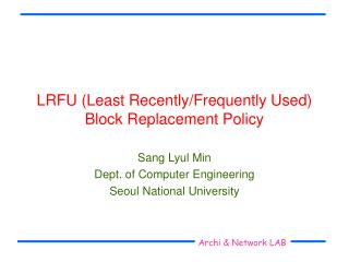
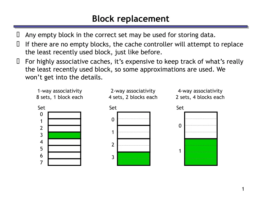
1-way associativity 8 sets, 1 block each 2-way associativity 4 sets, 2 blocks each 4-way associativity 2 sets, 4 blocks each Set Set Set 0 1 2 3 4 5 6 7 0 1 2 3 0 1 Block replacement • Any empty block in the correct set may be used for storing data. • If there are no empty blocks, the cache controller will attempt to replace the least recently used block, just like before. • For highly associative caches, it’s expensive to keep track of what’s really the least recently used block, so some approximations are used. We won’t get into the details.
LRU example • Assume a fully-associative cache with two blocks, which of the following memory references miss in the cache. • assume distinct addresses go to distinct blocks 0 Tags 1 LRU addresses -- -- 0 A B A C B A B
8-way 1 set, 8 blocks 1-way 8 sets, 1 block each 2-way 4 sets, 2 blocks each 4-way 2 sets, 4 blocks each Set Set Set Set 0 1 2 3 4 5 6 7 0 1 2 3 0 1 0 direct mapped fully associative Set associative caches are a general idea • By now you may have noticed the 1-way set associative cache is the same as a direct-mapped cache. • Similarly, if a cache has 2k blocks, a 2k-way set associative cache would be the same as a fully-associative cache.
Address (m bits) Block offset Tag Index (m-k-n) k Index Valid Tag Data Valid Tag Data 0 ... 2k 2n 2n = = 2-to-1 mux Hit 2n Data 2-way set associative cache implementation • How does an implementation of a 2-way cache compare with that of a fully-associative cache? • Only two comparators are needed. • The cache tags are a little shorter too.
Summary of What We Saw So Far • Larger block sizes can take advantage of spatial locality by loading data from not just one address, but also nearby addresses, into the cache. • Associative caches assign each memory address to a particular set within the cache, but not to any specific block within that set. • Set sizes range from 1 (direct-mapped) to 2k (fully associative). • Larger sets and higher associativity lead to fewer cache conflicts and lower miss rates, but they also increase the hardware cost. • In practice, 2-way through 16-way set-associative caches strike a good balance between lower miss rates and higher costs. • Next we’ll discuss the issue of writing data to a cache. We will also talk more about measuring cache performance.
Four important questions 1. When we copy a block of data from main memory to the cache, where exactly should we put it? 2. How can we tell if a word is already in the cache, or if it has to be fetched from main memory first? 3. Eventually, the small cache memory might fill up. To load a new block from main RAM, we’d have to replace one of the existing blocks in the cache... which one? 4. How can write operations be handled by the memory system? • Previous lectures answered the first 3. Today, we consider the 4th.
Index V Tag Data Address Data ... 110 ... ... 1101 0110 ... 1 11010 42803 42803 Mem[214] = 21763 Index V Tag Data Address Data ... 1101 0110 ... ... 110 ... 1 11010 21763 42803 Writing to a cache • Writing to a cache raises several additional issues. • First, let’s assume that the address we want to write to is already loaded in the cache. We’ll assume a simple direct-mapped cache. • If we write a new value to that address, we can store the new data in the cache, and avoid an expensive main memory access.
Index V Tag Data Address Data ... 110 ... ... 1101 0110 ... 1 11010 21763 42803 Inconsistent memory • But now the cache and memory contain different, inconsistent data! • How can we ensure that subsequent loads will return the right value? • This is also problematic if other devices are sharing the main memory, as in a multiprocessor system.
Mem[214] = 21763 Index V Tag Data Address Data ... 110 ... ... 1101 0110 ... 1 11010 21763 21763 Write-through caches • A write-through cache solves the inconsistency problem by forcing all writes to update both the cache and the main memory. • This is simple to implement and keeps the cache and memory consistent. • Why is this not so good?
Producer Buffer Consumer Write buffers • Write-through caches can result in slow writes, so processors typically include a write buffer, which queues pending writes to main memory and permits the CPU to continue. • Buffers are commonly used when two devices run at different speeds. • If a producer generates data too quickly for a consumer to handle, the extra data is stored in a buffer and the producer can continue on with other tasks, without waiting for the consumer. • Conversely, if the producer slows down, the consumer can continue running at full speed as long as there is excess data in the buffer. • For us, the producer is the CPU and the consumer is the main memory.
Write-back caches • In a write-back cache, the memory is not updated until the cache block needs to be replaced (e.g., when loading data into a full cache set). • For example, we might write some data to the cache at first, leaving it inconsistent with the main memory as shown before. • The cache block is marked “dirty” to indicate this inconsistency • Subsequent reads to the same memory address will be serviced by the cache, which contains the correct, updated data. Mem[214] = 21763 Index V Dirty Tag Data Address Data ... 110 ... 1000 1110 1101 0110 ... 1225 1 1 11010 21763 42803
Dirty V 1 1 Dirty V 1 0 Finishing the write back • We don’t need to store the new value back to main memory unless the cache block gets replaced. • For example, on a read from Mem[142], which maps to the same cache block, the modified cache contents will first be written to main memory. • Only then can the cache block be replaced with data from address 142. Tag Data Address Data Index 1000 1110 1101 0110 ... 1225 ... 110 ... 11010 21763 21763 Tag Data Address Data Index 1000 1110 1101 0110 ... 1225 ... 110 ... 10001 1225 21763
Write-back cache discussion • Each block in a write-back cache needs a dirty bit to indicate whether or not it must be saved to main memory before being replaced—otherwise we might perform unnecessary writebacks. • Notice the penalty for the main memory access will not be applied until the execution of some subsequent instruction following the write. • In our example, the write to Mem[214] affected only the cache. • But the load from Mem[142] resulted in two memory accesses: one to save data to address 214, and one to load data from address 142. • The write can be “buffered” as was shown in write-through. • The advantage of write-back caches is that not all write operations need to access main memory, as with write-through caches. • If a single address is frequently written to, then it doesn’t pay to keep writing that data through to main memory. • If several bytes within the same cache block are modified, they will only force one memory write operation at write-back time.
Index V Tag Data Address Data ... 110 ... ... 1101 0110 ... 1 00010 123456 6378 Write misses • A second scenario is if we try to write to an address that is not already contained in the cache; this is called a write miss. • Let’s say we want to store 21763 into Mem[1101 0110] but we find that address is not currently in the cache. • When we update Mem[1101 0110], should we also load it into the cache?
Mem[214] = 21763 Address Data Index V Tag Data ... 1101 0110 ... ... 110 ... 21763 1 00010 123456 Write around caches (a.k.a. write-no-allocate) • With a write around policy, the write operation goes directly to main memory without affecting the cache.
Mem[214] = 21763 Address Data Index V Tag Data ... 1101 0110 ... ... 110 ... 21763 1 00010 123456 Write around caches (a.k.a. write-no-allocate) • With a write around policy, the write operation goes directly to main memory without affecting the cache. • This is good when data is written but not immediately used again, in which case there’s no point to load it into the cache yet. for (int i = 0; i < SIZE; i++) a[i] = i;
Mem[214] = 21763 Index V Tag Data Address Data ... 110 ... ... 1101 0110 ... 1 11010 21763 21763 Allocate on write • An allocate on write strategy would instead load the newly written data into the cache. • If that data is needed again soon, it will be available in the cache.
Which is it? • Given the following trace of accesses, can you determine whether the cache is write-allocate or write-no-allocate? • Assume A and B are distinct, and can be in the cache simultaneously. Miss Load A Miss Store B Hit Store A Hit Load A Miss Load B Hit Load B Hit Load A
A few notes about the midterm int a[128]; int i = 3; int b, c, d … b = a[i]; c = *(a+i); d = *(a+i*4); int z = 19; int t, w; t = z >> 2; w = t << 2; (is z = w ?) div mul Hi/Lo registers
Main Memory L2 cache CPU L1 cache First Observations • Split Instruction/Data caches: • Pro: No structural hazard between IF & MEM stages • A single-ported unified cache stalls fetch during load or store • Con: Static partitioning of cache between instructions & data • Bad if working sets unequal: e.g.,code/DATA or CODE/data • Cache Hierarchies: • Trade-off between access time & hit rate • L1 cache can focus on fast access time (okay hit rate) • L2 cache can focus on good hit rate (okay access time) • Such hierarchical design is another “big idea” • We’ll see this in section.
Main Memory L2 cache CPU L1 cache Opteron Vital Statistics • L1 Caches: Instruction & Data • 64 kB • 64 byte blocks • 2-way set associative • 2 cycle access time • L2 Cache: • 1 MB • 64 byte blocks • 4-way set associative • 16 cycle access time (total, not just miss penalty) • Memory • 200+ cycle access time
Comparing cache organizations • Like many architectural features, caches are evaluated experimentally. • As always, performance depends on the actual instruction mix, since different programs will have different memory access patterns. • Simulating or executing real applications is the most accurate way to measure performance characteristics. • The graphs on the next few slides illustrate the simulated miss rates for several different cache designs. • Again lower miss rates are generally better, but remember that the miss rate is just one component of average memory access time and execution time. • You’ll probably do some cache simulations if you take CS433.
12% 9% Miss rate 6% 3% 0% One-way Two-way Four-way Eight-way Associativity Associativity tradeoffs and miss rates • As we saw last time, higher associativity means more complex hardware. • But a highly-associative cache will also exhibit a lower miss rate. • Each set has more blocks, so there’s less chance of a conflict between two addresses which both belong in the same set. • Overall, this will reduce AMAT and memory stall cycles. • The textbook shows the miss rates decreasing as the associativity increases.
15% 12% 9% 1 KB Miss rate 2 KB 4 KB 6% 8 KB 3% 0% One-way Two-way Four-way Eight-way Associativity Cache size and miss rates • The cache size also has a significant impact on performance. • The larger a cache is, the less chance there will be of a conflict. • Again this means the miss rate decreases, so the AMAT and number of memory stall cycles also decrease. • The complete Figure 7.29 depicts the miss rate as a function of both the cache size and its associativity.
40% 35% 30% 1 KB 25% 8 KB 20% Miss rate 16 KB 64 KB 15% 10% 5% 0% 4 16 64 256 Block size (bytes) Block size and miss rates • Finally, Figure 7.12 on p. 559 shows miss rates relative to the block size and overall cache size. • Smaller blocks do not take maximum advantage of spatial locality.
Memory and overall performance • How do cache hits and misses affect overall system performance? • Assuming a hit time of one CPU clock cycle, program execution will continue normally on a cache hit. (Our earlier computations always assumed one clock cycle for an instruction fetch or data access.) • For cache misses, we’ll assume the CPU must stall to wait for a load from main memory. • The total number of stall cycles depends on the number of cache misses and the miss penalty. Memory stall cycles = Memory accesses x miss rate x miss penalty • To include stalls due to cache misses in CPU performance equations, we have to add them to the “base” number of execution cycles. CPU time = (CPU execution cycles + Memory stall cycles) x Cycle time
Performance example • Assume that 33% of the instructions in a program are data accesses. The cache hit ratio is 97% and the hit time is one cycle, but the miss penalty is 20 cycles. Memory stall cycles = Memory accesses x Miss rate x Miss penalty = 0.33 I x 0.03 x 20 cycles = 0.2 I cycles • If I instructions are executed, then the number of wasted cycles will be 0.2 x I. This code is 1.2 times slower than a program with a “perfect” CPI of 1!
Memory systems are a bottleneck CPU time = (CPU execution cycles + Memory stall cycles) x Cycle time • Processor performance traditionally outpaces memory performance, so the memory system is often the system bottleneck. • For example, with a base CPI of 1, the CPU time from the last page is: CPU time = (I + 0.2 I) x Cycle time • What if we could double the CPU performance so the CPI becomes 0.5, but memory performance remained the same? CPU time = (0.5 I + 0.2 I) x Cycle time • The overall CPU time improves by just 1.2/0.7 = 1.7 times! • Refer back to Amdahl’s Law from textbook page 101. • Speeding up only part of a system has diminishing returns.
CPU Cache Main Memory Basic main memory design • There are some ways the main memory can be organized to reduce miss penalties and help with caching. • For some concrete examples, let’s assume the following three steps are taken when a cache needs to load data from the main memory. • It takes 1 cycle to send an address to the RAM. • There is a 15-cycle latency for each RAM access. • It takes 1 cycle to return data from the RAM. • In the setup shown here, the buses from the CPU to the cache and from the cache to RAM are all one word wide. • If the cache has one-word blocks, then filling a block from RAM (i.e., the miss penalty) would take 17 cycles. 1 + 15 + 1 = 17 clock cycles • The cache controller has to send the desired address to the RAM, wait and receive the data.
CPU Cache Main Memory Miss penalties for larger cache blocks • If the cache has four-word blocks, then loading a single block would need four individual main memory accesses, and a miss penalty of 68 cycles! 4 x (1 + 15 + 1) = 68 clock cycles
CPU Cache Main Memory A wider memory • A simple way to decrease the miss penalty is to widen the memory and its interface to the cache, so we can read multiple words from RAM in one shot. • If we could read four words from the memory at once, a four-word cache load would need just 17 cycles. 1 + 15 + 1 = 17 cycles • The disadvantage is the cost of the wider buses—each additional bit of memory width requires another connection to the cache.
CPU Cache Main Memory Bank 0 Bank 1 Bank 2 Bank 3 An interleaved memory • Another approach is to interleave the memory, or split it into “banks” that can be accessed individually. • The main benefit is overlapping the latencies of accessing each word. • For example, if our main memory has four banks, each one byte wide, then we could load four bytes into a cache block in just 20 cycles. 1 + 15 + (4 x 1) = 20 cycles • Our buses are still one byte wide here, so four cycles are needed to transfer data to the caches. • This is cheaper than implementing a four-byte bus, but not too much slower.
Clock cycles Load word 1 Load word 2 Load word 3 Load word 4 15 cycles Interleaved memory accesses • Here is a diagram to show how the memory accesses can be interleaved. • The magenta cycles represent sending an address to a memory bank. • Each memory bank has a 15-cycle latency, and it takes another cycle (shown in blue) to return data from the memory. • This is the same basic idea as pipelining! • As soon as we request data from one memory bank, we can go ahead and request data from another bank as well. • Each individual load takes 17 clock cycles, but four overlapped loads require just 20 cycles.
Which is better? • Increasing block size can improve hit rate (due to spatial locality), but transfer time increases. Which cache configuration would be better? • Assume both caches have single cycle hit times. Memory accesses take 15 cycles, and the memory bus is 8-bytes wide: • i.e., an 16-byte memory access takes 18 cycles: 1 (send address) + 15 (memory access) + 2 (two 8-byte transfers) recall: AMAT = Hit time + (Miss rate x Miss penalty)
Which is better? • Increasing block size can improve hit rate (due to spatial locality), but transfer time increases. Which cache configuration would be better? • Assume both caches have single cycle hit times. Memory accesses take 15 cycles, and the memory bus is 8-bytes wide: • i.e., an 16-byte memory access takes 18 cycles: 1 (send address) + 15 (memory access) + 2 (two 8-byte transfers) recall: AMAT = Hit time + (Miss rate x Miss penalty) Cache #1: Miss Penalty = 1 + 15 + 32B/8B = 20 cycles AMAT = 1 + (.05 * 20) = 2 Cache #2: Miss Penalty = 1 + 15 + 64B/8B = 24 cycles AMAT = 1 + (.04 * 24) = ~1.96
Summary • Writing to a cache poses a couple of interesting issues. • Write-through and write-back policies keep the cache consistent with main memory in different ways for write hits. • Write-around and allocate-on-write are two strategies to handle write misses, differing in whether updated data is loaded into the cache. • Memory system performance depends upon the cache hit time, miss rate and miss penalty, as well as the actual program being executed. • We can use these numbers to find the average memory access time. • We can also revise our CPU time formula to include stall cycles. AMAT = Hit time + (Miss rate x Miss penalty) Memory stall cycles = Memory accesses x miss rate x miss penalty CPU time = (CPU execution cycles + Memory stall cycles) x Cycle time • The organization of a memory system affects its performance. • The cache size, block size, and associativity affect the miss rate. • We can organize the main memory to help reduce miss penalties. For example, interleaved memory supports pipelined data accesses.