Download
1 / 33
330 likes | 414 Views
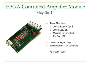
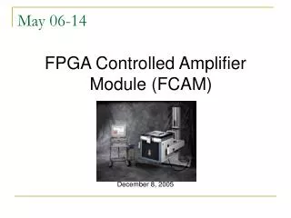
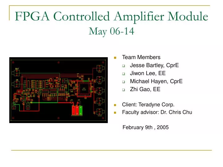
FPGA Controlled Amplifier Module May 06-14. Team Members Jesse Bartley, CprE Ji w on Lee, EE Michael Hayen, CprE Zhi Gao, EE Client: Teradyne Corp. Faculty advisor: Dr. Chris Chu February 9th , 2005. Presentation Outline. Introductory Materials Project Activity Description

E N D
FPGA Controlled Amplifier ModuleMay 06-14 • Team Members • Jesse Bartley, CprE • Jiwon Lee, EE • Michael Hayen, CprE • Zhi Gao, EE • Client: Teradyne Corp. • Faculty advisor: Dr. Chris Chu February 9th , 2005
Presentation Outline • Introductory Materials • Project Activity Description • Resources and Schedules • Closing Materials May 06-14
List of Terms and Definitions • Bill of Materials – List of Components and their cost • DAC – Conversion of a digital signal to an analog sampled signal • DC-offset– given signal source does not have the correct 0-crossing but shifted down or up. • FPGA – Field programmable gate arrays, allows us to control some the circuits automatically • Gain – The ratio of the output amplitude to the input amplitude • HDL – Hardware Description Language • Noise – Undesired interference in signals • Spectrum Analyzer – A computer-based tool that analyzes signals in the frequency domain • THD – Total harmonic distortion, the ratio between the powers of all harmonic frequencies above the fundamental frequency May 06-14
Acknowledgement • Teradyne Corporation • Jacob Mertz • Ramon De La Cruz • Steven Miller • Additional Help • Jason Boyd • Dr. Robert Weber May 06-14
Problem Statement & Approach • Problem statement: • To complete and test the FPGA controlled Amplifier for PC based Spectrum Analyzer developed by previous team • Approach: • Understand existing design • Board assembly and bring-up • Make detailed test plan • Perform and document tests May 06-14
Operating Environment & Treatment Cautions • A climate-controlled laboratory (At room temperature with low humidity) • ESD (Electro Static Discharge) • Safe place (locker) to keep equipments May 06-14
Intended Users & Uses • The primary users: • Engineers of the Teradyne Corporation • Possible derivative could be used outside Teradyne in the future. • The product function: • As a pre-amplifier for the signal input to a PC based spectrum analyzer device. • PC based spectrum analyzer was designed by previous phase May 06-14
Assumptions and Limitations • Assumptions • The end product will not be sold to other companies. • The design provided by the previous team is valid. • Necessary equipment will be available. • Limitations • Equipments must be available on campus • The design must meet specifications May 06-14
DC — 1kHz Input +/- 5 volts 6, 20, 40, 60 +/- 10 volts 0.05 dB < - 105 dB Total 1.5 nV/rtHz Input Voltage Available Max Output Freq Response Harmonic > 1kHz - 20 kHz +/- 5 volts 6, 20, 40, 60 +/- 10 volts 0.05 dB < - 95 dB 1.5 nV/rtHz Frequency Range Gain Settings Voltage Flatness Distortion Noise > 20kHz - 100kHz +/- 2.5 volts 6, 20, 40 +/- 5 volts 0.10 dB < -85 dB 2.5 nV/rtHz Range (Volts) (dB) (Volts) (dB) (dB) (nV/rtHz) > 100kHz - 1MHz +/- 2.5 volts 6, 20, 40 +/- 5 volts 0.10 dB < - 80 dB 3.5 nV/rtHz > 1MHz - 10MHz +/- 2.5 volts 6, 20, 40 +/- 5 volts 0.10 dB < - 70 dB 3.5 nV/rtHz > 10MHz - 20MHz +/- 2.5 volts 6, 20 +/- 5 volts 0.10 dB < -65 dB 3.5 nV/rtHz > 20MHz - 50MHz +/- 1.0 volts 6, 20 +/- 2.0 volts 1.00 dB < -50 dB 5.0 nV/rtHz > 50MHz - 100MHz +/- 1.0 volts 6, 20 +/- 2.0 volts 2.10 dB < -40 dB 5.0 nV/rtHz Design Specifications May 06-14
End Product & Other Deliverables • A fully functional and tested design • A functioning prototype • Complete test plans • A full test report • Technical documentation on the design May 06-14
Previous Accomplishments • FPGA code • General Design • Documentation of progress • Design Schematic • Bill of Materials • Partial assembly May 06-14
Present Accomplishments & Future Required Activities • Present Accomplishments: • Order missing parts • Board Assembly • Research and Verification • Re-vamp FPGA code • Make detailed test plan • Remaining Activities • Test amplifier • Produce test reports • Deliver finalized design May 06-14
Approaches Considered and one used • Approaches considered: • Manual testing and calculation • LabVIEW automated testing and Excel calculation • Choice: LabVIEW automated testing • Repeatability • Self documentation • Speed/efficiency • Extra research required May 06-14
Project Definition Activities • Goals of this project: • Research & verify the previous design • Meet the specifications • Board Assembly • Make a detailed test plan • Testing • Documents all processes May 06-14
Research Activities • Study previous team’s design • Pspice simulation • Point of reference during bring up • Determine new specifications • Determine causes of problems found • Test methodologies • Noise • THD • LabVIEW May 06-14
Design Activities • Verification of design • DC Offset Correction • Operational Amplifier • Tests design • DC Offset Correction verification tests • Amplifier performance tests • Integration testing May 06-14
Implementation Activities • Errors on the PCB were fixed • New Pspice Simulation was developed • Specifications were adjusted • Test strategy was developed according to Client suggestions May 06-14
Testing Activities • Location Microwave Engineering Lab (Room 344, Durham) • Specification • Pre-determined by the Client • Methodology • LabVIEW Automated • Testing Accuracy • Must ensure that equipment is accurate enough • Tolerance was calculated from different specifications of components May 06-14
Testing Activities • Specifications needed to be tested • Amplification Bandwidth (10Hz – 100MHz) • Noise density • THD (Total Harmonic Distortion) • DC-Offset correction accuracy • DC-Offset correction calibration time May 06-14
Testing Activities • List of tests • Amplifier gain test • Total harmonic distortion test • Circuit noise test • Amplifier gain flatness and bandwidth test • VHDL code behavior test • DAC control test • Offset calibration test • Offset correction verification test May 06-14
Other Activities • Choosing equipment • Finding options • Researching specifications • Getting access • Poster May 06-14
Personnel Effort Requirements May 06-14
Financial Requirement May 06-14
Project Schedules May 06-14
Deliverable Schedules May 06-14
Project Evaluation May 06-14
Commercialization • Further modifications necessary for commercialization • Thorough testing helps improve viability • Needs to be packaged with PC based spectrum analyzer for commercialization • Price to be determined • Potential Market • Small technology companies May 06-14
Additional Work • Recommended additions • Full automation may be achieved • Frequency response calibration • PC control may be added to the product • Future integration with Spectrum Analyzer May 06-14
Lessons Learned • Experience gained • Test design • Test implementation • Team Work • Working with an outside client • Following schedules May 06-14
Risk and Management • Test results may be unexpected • Conduct proper trouble shooting • Loss of a team member (Did not encounter) • Work cooperatively • Good communication • Hardware Damage • Quick replacement and backup board • Specifications are not practical • Define new specifications (with client input) May 06-14
Closing Summary • This Team’s Tasks • Assemble the prototype • Develop FPGA code • Test the product • Document all details of the process • Project will make contribution • Teradyne • Integrated circuit industry • The team will received the following benefits: • Technical knowledge • Team work • Real industry project • Overall, this project will benefit both the client and the team May 06-14
Questions ??? May 06-14