FPGA Circuits
FPGA Circuits. A simple FPGA model Full-adder realization Demos. Presentation References. Altera Training Course “Designing With Quartus-II” Altera Training Course “Migrating ASIC Designs to FPGA” Altera Training Course “Introduction to Verilog”

FPGA Circuits
E N D
Presentation Transcript
FPGA Circuits • A simple FPGA model • Full-adder realization • Demos
Presentation References • Altera Training Course “Designing With Quartus-II” • Altera Training Course “Migrating ASIC Designs to FPGA” • Altera Training Course “Introduction to Verilog” • S. Brown and J. Rose, “Architecture of FPGAs and CPLDs: A Tutorial”, Department of Electrical and Computer Engineering, University of Toronto • Online academic notes “pld devices.pdf”
What are Programmable Chips? • As compared to hard-wired chips, programmable chips can be customized as per needs of the user by programming • This convenience, coupled with the option of re-programming in case of problems, makes the programmable chips very attractive • Other benefits include instant turnaround, low starting cost and low risk
What are Programmable Chips? • As compared to programmable chips, ASIC (Application Specific Integrated Circuit) has a longer design cycle and costlier ECO (Engineering Change Order) • Still, ASIC has its own market due to the added benefit of faster performance and lower cost if produced in high volume • Programmable chips are good for medium to low volume products. If you need more than 10,000 chips, go for ASIC or hard copy
What is Available? • PLA (Programmable Logic Array) is a simple field programmable chip that has an AND plane followed by an OR plane. It is based on the fact that any logical function can be written in SOP (Sum of Products) form thus any function can be implemented by AND gates generating products which feed to an OR gate that sums them up
Example • F(A,B,C) = A’B’C + AB’C + ABC • How will it be implemented in a PLA?
What is Available? • CPLD (Complex Programmable Logic Device) consists of multiple PLA blocks that are interconnected to realize larger digital systems • FPGA (Field Programmable Gate Array) has narrower logic choices and more memory elements. LUT (Lookup Table) may replace actual logic gates
Lookup Table • A LUT (Lookup table) is a one bit wide memory array • A 4-input AND gate is replaced by a LUT that has four address inputs and one single bit output with 16 one bit locations • Location 15 would have a logic value ‘1’ stored, all others would be zero • LUT’s can be programmed and reprogrammed to change the logical function implemented
ADDRESS ADDRESS (BINARY) CONTENTS 0 0000 0 1 0001 1 2 0010 1 3 0011 0 4 0100 1 5 0101 0 6 0110 0 7 0111 1 8 1000 1 9 1001 0 10 1010 0 11 1011 1 12 1100 0 13 1101 1 14 1110 1 15 1111 0 LUT FOR 4-INPUT EVEN PARITY GENERATOR
PLD Design Flow Design Specification Design Entry/RTL Coding - Behavioral or Structural Description of Design RTL Simulation -Functional Simulation - Verify Logic Model & Data Flow (No Timing Delays) M512 LE Synthesis - Translate Design into Device Specific Primitives - Optimization to Meet Required Area & Performance Constraints M4K I/O Place & Route - Map Primitives to Specific Locations inside Target Technology with Reference to Area & Performance Constraints - Specify Routing Resources to Be Used
PLD Design Flow Timing Analysis - Verify Performance Specifications Were Met - Static Timing Analysis tclk Gate Level Simulation -Timing Simulation - Verify Design Will Work in Target Technology PC Board Simulation & Test -Simulate Board Design - Program & Test Device on Board
Why FPGA? • FPGA chips handle dense logic and memory elements offering very high logic capacity • Uncommitted logic blocks are replicated in an FPGA with interconnects and I/O blocks
Quick Logic Actel Altera Atmel DynaChip Lucent Motorola Vantis Xilinx Gate Field I-Cube Lattix Aptix Antifuse-FPGA SRAM-FPGA Flash-FPGA FPIDs Manufacturers and types of FPGAs
Meet Altera: Our Industry Contact • Programmable Devices • Design Software • Intellectual Property (IP)
Introduction to Altera Devices • Programmable Logic Families • High & Medium Density FPGAs • Stratix™ II, Stratix, APEX™ II, APEX 20K, & FLEX® 10K • Low-Cost FPGAs • Cyclone™ & ACEX® 1K • FPGAs with Clock Data Recovery • Stratix GX & Mercury™ • CPLDs • MAX® 7000 & MAX 3000 • Embedded Processor Solutions • Nios™, ExcaliburT™ • Configuration Devices • EPC
Software & Development Tools: Quartus II Stratix II, Stratix, Stratix GX, Cyclone, APEX II, APEX 20K/E/C, Excalibur, & Mercury Devices FLEX 10K/A/E, ACEX 1K, FLEX 6000, MAX 7000S/AE/B, MAX 3000A Devices Quartus II Web Edition Free Version Not All Features & Devices Included MAX+PLUS® II All FLEX, ACEX, & MAX Devices Introduction to AlteraDesign Software
Altera University Program • Under our membership contract, we subscribe to Quartus design software and serve its three floating licenses • The number of licenses will be increased based on growth in usage • Altera plans to send us Cyclone FPGA programming boards and a few FPGA chips • Cyclone is the lowest cost FPGA family ($3-$7 per chip) and includes maximum of 20K logic elements and 300Kbits of memory • Stratix is the highest density FPGA with max of 80K logic elements, 10Mbits memory, PLL, DSP and DDR interface blocks
Quartus II Development System • Fully-Integrated Design Tool • Multiple Design Entry Methods • Logic Synthesis • Place & Route • Simulation • Timing & Power Analysis • Device Programming
More Features • MegaWizard® & SOPC Builder Design Tools • LogicLock™ Optimization Tool • NativeLink® 3rd-Party EDA Tool Integration • Integrated Embedded Software Development • SignalTap® II & SignalProbe™ Debug Tools • Windows, Solaris, HPUX, & Linux Support • Node-Locked & Network Licensing Options • Revision Control Interface
Nios: The processor in software • Altera has implemented a full 16/32 bit RISC processor in HDL (Hardware Description Language) • Nios is a processor core that is available as a megafunction in Quartus and it can be targeted for all Altera FPGA’s • Programs can be written for Nios using open GNU pro tools
Megafunctions • Pre-Made Design Blocks • Ex. Multiply-Accumulate, PLL, Double-Data Rate, Nios • Benefits • Accelerate Design Entry • Pre-Optimized for Altera Architecture • Add Flexibility • Two Types • Altera-Specific Megafunctions • Library of Paramerterized Modules (LPMs) • Industry Standard Logic Functions
MegaWizard Plug-In Manager • Eases Implementation of Megafunctions & IP
MegaWizard Examples PLL Multiply-Add Double-Data Rate
FPGA Design Cycle with Altera Quartus Tool • Define a new project and enter the design using VHDL, Verilog or AHDL languages. Design can also be entered using Schematic diagrams that can be translated to any HDL • Compile and simulate the design. Find and fix timing violations. Get power consumption estimates and perform synthesis • Download the design to FPGA using a programmer board
Downloading the Design • Once we verify FPGA based design, the design tool allows us to download the program to an FPGA chip • Designs can be downloaded using parallel port or USB cables • Designs can also be downloaded via the Internet to a target device
Hard Copy • Once an FPGA design is verified, validated and used successfully, there is an option to migrate it to structured ASIC • This option is known as Hard Copy • Using hard copy, FPGA design can be migrated to hard-wired design removing all configuration circuitry and programmability so that the target chip can be produced in high volume • Hard copied chip uses 40% less power than FPGA and the internal delays are reduced
A simple FPGA model • The abstract FPGA device is made up of a regular two-dimensional array of cells • Each cell has four faces • Signals can connect the face of the tile and can be individually configured for input or output
FPGA structure • Additionally to the previous array express buses are needed • The most modern FPGA architectures provide some kind of special long distance routing • The cell architecture is comprised of a function unit thatcan assume any two input logic function, a 2:1multiplexer, or a D-type flip-flop • Reset andclear signals are routed to each cell • The function unit canalso implement an inverter as well as the identity function
Logic functions • In principle: • the function unit could realize any three inputlogic function • However: • it is not very common forcurrent FPGAs to provide cells with such three inputfunctions • although some do allow two 2-input gates to berealised with separate outputs • Cells which can realize 2:1multiplexers are becoming more widespread • this isthe only kind of three input function that we allow • Inpractise: • the third signal will come not from aneighbouring cell • but from a local or global express bussignal
Cell level connections • Each output port can be driven by the output of thefunction unit • or an input from any other face
Full-adder • Signal flow through full-adder
Implementation of the half-adder • (a) half-adder top level • (b) implementation
A full-adder realization I • The circuit adds A and B with carry in to produce sum and carry out • The B input is split into two paths by the bottom left cell
A full-adder realization II • This can be done by realizing the identity function in the cell and connecting the South and West ports to the cell’s function unit output • Both exclusive-or gates take their inputs from the North and East ports and deliver the exclusive-or of these inputs on the West face • The South port of these cells is connected to the North input (shown as a grey line) allowing the carry in to be propagated to the cell below
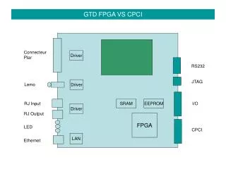
FPGA /ATMEL 6000 series Features • High-performance • Up to 204 User I/Os • Thousands of Registers • Cache Logic® Design • Low Voltage and Standard Voltage Operation • Automatic Component Generators • Very Low-power Consumption • Programmable Clock Options • Independently Configurable I/O (PCI Compatible) • Easy Migration to Atmel Gate Arrays for High Volume Production
FPGA /ATMEL 6000 series • AT6000 Series SRAM-Based Field Programmable Gate Arrays (FPGAs) are ideal for use as reconfigurable coprocessors and implementing compute intensive logic • Supporting system speeds greater than 100 MHz and using a typical operating current of 15 to 170 mA, AT6000 Series devices are ideal for high-speed, compute-intensive designs • The patented AT6000 Series architecture employs a symmetrical grid of small yet powerful cells connected to a flexible busing network. Independently controlled clocks and resets govern every column of cells • The array is surrounded by programmable I/O
FPGA /ATMEL 6000 series • Devices range in size from 4,000 to 30,000 usable gates, and 1024 to 6400 registers. Pin locations are consistent throughout the AT6000 Series for easy design migration • AT6000 Series FPGAs utilize a reliable 0.6 mm single poly, double-metal CMOS process and are 100% factory tested • The cell’s small size leads to arrays with large numbers of cells, greatly multiplying the functionality in each cell • A simple, high-speed busing network provides fast, efficient communication over medium and long distances.
ATMEL 6000 /The Symmetrical Array • At the heart of the Atmel architecture is a symmetrical array of identical cells • The array is continuous and completely uninterrupted from one edge to the other, except for bus repeaters spaced every eight cells • In addition to logic and storage, cells can also be used as wires to connect functions together over short distancesand are useful for routing in tight spaces
ATMEL 6000 /The Busing Network • There are two kinds of buses: local and express • Local buses are the link between the array of cells and the busing network • There are two local buses North-South 1 and 2 for every column of cells, and two local buses East-West 1 and 2 for every row of cells • Express buses are not connected directly to cells, and thus provide higher speeds • They are the fastest way to cover long, straight-line distances within the array • Each express bus is paired with a local bus, so there are two express buses for every column and two express buses for every row of cells
ATMEL 6000/The Cell Structure • The Atmel cell can be programmed to perform all the logic and wiring functions needed to implement any digital circuit • To read a local bus, the pass gate for that bus is turned on and the three input multiplexer is set accordingly • To write to a local bus, the pass gate for that bus and the pass gate for the associated tristate driver are both turned on • The operations of reading, writing and turning are subject to the restriction that each bus can be involved in no more than a single operation Reference: www.gaw.ru/pdf/Atmel/DOC0264.PDF
ATMEL AVR Modules The Development environment is composed of: • The main board • Including Atmel AVR microcontroller • Its types: • Atmel Atmega128/64 development main board • Atmel Atmega16/32 development main board • Atmel Atmega8 development main board • Atmel Attiny15L development main board • Peripherals • They can be connected with standard strip line to the main board
Xilinx: SRAM-FPGA • Several times reprogrammable • Xilinx Virtex Architecture: • Consisting of more than 10mio cells • 1 module consisting of: - I/O-Blocks (IOB) - Block-Select-RAM - Combinatorial Logic Blocks (CLB) - 2 Slices - 2 Logic Cells - 2 Look-up tables with 4 inputs, 2 flip-flops, carry logic and routing
LUT – Look-up table • Programmed part of CLB • 4 Inputs, 1 Output • Each LUT contains 16x1 Bit memory • Conditioned to give for each combination at the input a value of a logic function at the output • Get the program at „Switch-ON“ from Block-RAM • Program is erased after „Switch-OFF“