Download
1 / 27
280 likes | 664 Views
KITPC2010. Semiconductor and Graphene Spintronics. Spintronics applications : spin FET role of interface on spin-polarized current in FM/SC, FM/graphene junctions. Jun-ichiro Inoue Nagoya University, Japan. Collaborators. Syuta Honda PD, Kansai University Yamamura T. Hiraiwa R. Sato

E N D
KITPC2010 Semiconductor and Graphene Spintronics Spintronics applications : spin FET role of interface on spin-polarized current in FM/SC, FM/graphene junctions Jun-ichiro Inoue Nagoya University, Japan
Collaborators • Syuta Honda • PD, Kansai University • Yamamura • T. Hiraiwa • R. Sato • MC students, Nagoya University, Japan • Hiroyoshi Itoh • Asc. Prof., Kansai University, Japan • (computer codes)
Outline • Introduction - role of junction interface on GMR, TMR - spin MOSFET and issues for SC, graphene • Spin injection and MR in spin MOSFET - some experiments - role of Schottky barrier on spin polarized current • Two-terminal lateral graphene junctions - a simple model for MR - band mixing at interface; effects on DPs - more realistic models
Spintronics • Usage of both charge and spin of electrons • Phenomana and applications - GMR, TMR, CIMS sensors, MRAM • - GMR: spin dependent scattering at interfaces • - TMR: matching/mismatching of band symmetrybetween • two electrodes (D1 symmetry) • Semiconductor spintronics - spin FET, spin MOSFET with semiconductors - or graphene
gate 2DEG with SOI FM Spin MOSFET • Conventional MOSFET • - Unipolar transistor • Spin transistor - Monsma et al.: hot electron spin transistor - Datta-Das: gate control of SOI • Sugawara-Tanaka • - Spin MOSFET with half-metals • - logic + memory device • Many proposals - Flatté-Vignale: Unipolar spin diodes &transistors - psuedospintronics, valleytronics in graphene
Electrons gate FM Issues and materials • Spin injection, transport and detection • Materials - Si: promising candidate, compatible with Si CMOS technology, weak spin-orbit interaction (SOI) - GaAs: high mobility, gate controllable SOI many experiments on spin injection - Graphene: high mobility, weak SOI long spin diffusion length, • Role of interface on spin-dep. Transport in GaAs and graphene junctions
Some Experiments • Spin injection into GaAs: • - Schottky barrier or tunnel barrier • - spin polarization 40 ~ 50 % • - optical detection • - GaMnAs as spin injector • high ratio only at low T • e.g. O. M. van’t Erve et al., APL 84, 4334 (2004) X. Jiang et al., PRL94, 56601 (2005) Van Dorpe et al. PRB (2005) • Spin injection into Si: • - spin polarization 10~20% • B. T. Jonker et al., Nature (2007)
P>0 P<0 e- Imaging of spin injection • Positive spin accumulation in GaAs • - Lateral Fe/GaAs/Fe, Kerr effect • Negative spin polarization in current from GaAs to Fe • Negative spin polarization - Fe/GaAs/Fe junctions, negative TMR • Moser et al., APL 89, 162106 (2006) • -Current induced by photo-excited electrons Kurebayashi et al., APL 91, 102114 (2007) S. A. Crooker et al., Science 309, 2192 (2005) • see also: Kotissek et al., Nat. phys. 3, 872 (2007) • Lou et al., Nat. phys. 3 193 (2007)
Conduction band EC IRS (Schokley state) Valence band Fe GaAs ↑spin EC spin Electronic states at interface of GaAs • Band structure of GaAs at interface • IRSs mix with Fe bands • - ↑spin bands; strong mixing • - ↓spin bands; weak mixing • due to band symmetry
2 As contact Ga contact As contact Ga contact spin GaAs bulk 1 spin DS EC spin DOS [eV-1] As Fe 0 200 ML n-GaAs Fe -1 spin EF -2 0 2 Fe Ga E-EC [eV] Interfacial resonant states (IRSs) : local DOS Spin dependent IRSs appear in SB. ↓spin IRSs in Fe-As contact are sharp. Ls = 200ML, Ds = 0.5 eV Exp. barrier height ~ 0.49 – 0.44 eV
1 0.7 0.5 0.4 P 0 0.1 Fe GaAs DS=0.3eV -1 0 0.2 0.4 0.6 0.8 1 Bias [V] V Bias dependence of spin polarization Spin polarization of current becomes negative for small Schokley barrier height. Negative bias: Contribution from ↓spin IRSs Zero bias: large I↑ due to D1 band symmetry Shift of IRSs
G DOS spin spin spin spin 0.0 -8 4.0 0 Log G(k||)[e2/h] D(k||) [eV-1] Momentum resolved conductance G point (DS=0.3eV, Bias=0.3V) IRSs spread over whole Brillouin zone, but those near the G point contribute to the conductance due to small Fermi surface of GaAs assumed. Large P
1 DS Fe Fe Bias~0.0V IP GaAs IAP 0 [10-5] 3 Bias~0.6V MR 2 0 0.2 0.4 0.6 0.8 1 I [e2/h] AP D1 P↑ D1 P↓ 1 -1 0 Bias [V] 0 0.2 0.4 0.6 0.8 1 Bias [V] DS [eV] 0.75(without Schottky barrier) 0.80 1.0 Fe/GaAs/Fe tunnel junctions Fe –As contact Potential profile
Conductivity mismatch SOI (barrier resistivity) Summary of first part • Fe/GaAs with Schottky barrier and Fe/GaAs/Fe • - Interfacial resonant states are spin dependent and give • large positive and negative spin polarization. • Control of Schottky barreir is crucial. • several issues, - Conductivity mismatch vs spin relaxation by SOI • Semiclassical model by Fert-Jaffres (2001) for FM/I/SC/I/FM • - roughness • - stacking direction SC layer • - half-metallic electrodes • - spin injection into Si
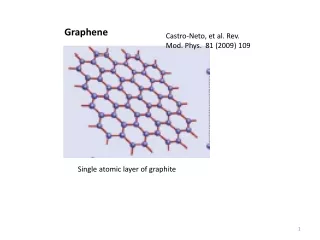
zig-zag edge p 2 armchair edge 0 E -2 y -4 Γ M K x E ky kx Graphene • Structure • 2-D Honeycomb lattice of C • Electronic states • s, px, py orbitals s bands • pz orbital p bands (zero-gap semiconductor) • Linear dispersion : Dirac points • Zero effective mass
Massless fermions • High mobility, low resistivity • New material for electronics Carbon atoms : light element • Weak spin-orbit interaction • Long spin diffusion length • application to spintronics 2-dimensionality • Gate control Characteristics of Graphene Possible applications Graphene transistor, spin-FET, terra-hertz wave, …
Top gate Graphene sheet FM Back gate FM/G/FM spin FET • Spin injection / MR effect • Current: on/off by gate – energy gap • nano-ribbon • bilayer graphene • Hydrogenation - graphane • Magnetization control • Fabrication method Exp. MR ratios a few % Non-local measurement Shiraishi’s group (2007)
10 10 DE DE [eV] E [eV] 0 0 0 1 2 3 Dirac point of Graphene k|| -10 -10 0 1 2 3 0 0 2 4 6 1 MR k|| G [e2/h] A simple model of MR • Matching of the conduction pass with DP E(k// ) for nano-ribbon with zigzag edge k//: momentum along the edge • MR appears when momentum matching is spin-dependent, and • when the band width of conduction band is narrow. • However, usual transition metal FM • Wide conduction band • no MR
1.0 0.8 0.6 Effective DP 0.4 a 0.2 0.01 0.05 L 0.0 0.1 2.09 2.10 2.11 0.3 G [e2/h] 0.5 1.0 k|| DP Tunnel barrier EF k// L=12[ML] MR in lateral FM/graphene/FM junctions • A single orbital tight-binding model + Kubo formula DP shifts due to contact with leads tunneling via states near DP Zigzag edge contact with electrodes (square lattice) W = ∞ tI=sps a
20ML Graphene s-□ s-□ k// 50ML 50ML probability density of graphene 0.0 1.0 Energy states of finite size junction Large band mixing Small band mixing E(k) k//
More details • Shift of DP with - Graphene length • - Band mixing at the contact • spin dependent G for FM electrodes
sp3 sp3d5 sp3d5 y L a a Zigzag edge z 4ML x Realistic contacts • Electrodes with fcc (111) lattice or triangular lattice wide overlap region between graphene and electrodes
0 10 0 10 G [e2/h/atm] -1 10 -1 1.0 10 0.5 -2 10 0.1 -2 10 0.05 LL=LR=1 -3 0.01 10 -3 LL=1 LR=400 10 LL=LR=400 -4 10 k// k// -4 10 -5 10 -5 2.07 2.08 2.09 2.1 2.11 10 1000 [ML] S+P 2.07 2.08 2.09 2.1 2.11 k// 5 [ML] LL [ML] LR [ML] Some preliminary results • Shift of DP with • - overlap of graphene and electrodes (triangular lattice) • - band mixing
GP GP 1 100 GAP GP 0.8 GP 103 10-2 GAP 0.6 MR G [e2/h] 10-4 102 G [e2/h] MR L 0.4 L=1000 10-6 K’ 0.2 W = ∞ 101 sp3 sp3d5 sp3d5 0 10-8 0 1000 2000 2.06 2.08 2.1 2.12 tI L [ML] tg k|| MR in bccFe/graphene/bccFe • Spin dependent band mixing at interface MR Bcc lattice on leads
1.0 Fe0.9Cr0.1 Fe0.7Co0.3 0.8 0.6 MR 0.4 0.2 Fe 0.0 -2.0 -1.0 0.0 1.0 2.0 DE [eV] MR in graphene junctions with Fe alloys • Materials dependence of MR – shifting the up spin band • Ferromagnetic alloys for lead • Change in the electronic state • of Fe alloys at the contact • matching of conduction channel becomes worse in up spin state
Summary of the second part • MR in FM/graphene/FM junctions • - Spin dependent shift of Dirac points appears • in zigzag edge contact. moderate MR effect • - MR can be large for some FM alloy electrodes. • Importance of electronic structure near the interface on spin injection and MR • Other effects unconsidered should be examined to • confirm the present results.
Interfacial hopping = tg J arm-chair edges zigzag edges k// G L (101 ML) L (100 ML) 0 J = 1.0 J = 1.0 -1 -2 Log G [e2/h / (atom spin)] -3 0.5 J = 0.5 -4 J = 0.1 -5 0.1 K -6 1.9 2 2.1 2.2 2.3 2.4 0 0.01 0.02 0.03 0.04 0.05 k// k// Zigzag edge vs Armchair edge • G of n-type graphene/graphene/n-graphene junctions