MuGFET
460 likes | 720 Views
MuGFET. First Time User Guide to MuGFET Mar. 28, 2008. Overview. Introduction Rappture input interface Rappture output interface Summary. Introduction-Structure. What is MuGFET ?. 1. The simulation tool for nano -scale FinFET structure. Double gate (AMD, IBM, Motorola).

MuGFET
E N D
Presentation Transcript
MuGFET First Time User Guide to MuGFET Mar. 28, 2008
Overview • Introduction • Rappture input interface • Rappture output interface • Summary
Introduction-Structure • What is MuGFET? • 1. The simulation tool for nano-scale FinFET structure • Double gate (AMD, IBM, Motorola) • Tri-gate or 3-D (Intel)
Introduction-Structure • 2. Simulator for nanowire structure
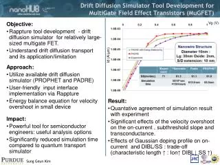
Introduction-Simulator • MuGFET uses existing simulation tool PROPHET and PADRE Available in nanohub.org Fast but rough – general partial differential eq. solver Comparison • PROPHET Slow but in detail – device oriented solver • PADRE Poisson equation Self consistent Drift-diffusion equation
Introduction-Purpose Purpose of MuGFET • Very convenient graphical user interface using Rappture Users don’t have to worry anything happened inside the simulator • Great flexibility with respect to structure and simulator • Drift-diffusion solver for relatively large nano-device • without full quantum mechanical calculation Fast and efficient
Overview • Introduction • Rappture input interface • Rappture output interface • Summary
Overall Procedure Device Type Device Structure Bias and Temperature Option Simulate
Example Loader Click! Choose
Example Loader Not changing any input of the example loaded, results come out from database without simulation
Example Loader If any input is changed from examples, full simulation will start
Device Type • Class : FinFET or Nanowire • Dimension 2D-Double Gate 3D-Triple Gate • Gate type : metal gate, poly gate
Device Structure Geometry in x, y, z
Device Structure • Geometry-X : Lateral Direction • Channel width • The width of silicon channel region • Oxide thickness • Left wall • Right wall • Poly gate thickness • Turned on if poly-gate type chosen in previous step The default device size is relatively large because this is a drift-diffusion type simulator. Specially, the cross section should be large compared to electron wave length so that quantum effect should not appear to use drift-diffusion equation.
Device Structure • Geometry-Y : Propagation Direction • Gate length • Not the channel length but the length of the gate electrode • Source length, drain length • Source extension length • The length how much the source is extended to the gate • Positive if the source is overlapped with the gate which means the gate goes over the source region • Negative if the source is underlapped with the gate which means the gate doesn’t go over the source region • The default : 0 • Drain extension length • Same as the source extension length
Device Structure • Geometry-Z • Vertical direction for 3D simulation • Channel height • The height of silicon channel region • Top_ox : oxide thickness on top of the channel • Substrate oxide thickness • SOI (Silicon on Insulator)
Geometry-X (Nanowire) radial direction The x-direction in nanowire is radial direction of the nanowire
Geometry-Y (Nanowire) The y-directional structure in nanowire configuration is same as that in finFET
Gaussian Doping • Gaussian Doping • Gaussian doping flag • Check “yes” if you want to build Gaussian doping profile • Characteristic length for source • The length from source and channel boundary to where the value of Gaussian doping is at its half • Characteristic length for drain • The length from drain and channel boundary to where the value of Gaussian doping is at its half • Penetration into oxide • The length how much the Gaussian doping penetrates into oxide region
Bias and Temperature Gate : Id-Vg plot for each Vd Drain: Id-Vd plot for each Vg
Options Options for PADRE Options for PROPHET
Overview • Introduction • Rappture input interface • Rappture output interface • Summary
p-FinFET 45nmX30nm Double Gate - IV Curve PROPHET and PADRE result comparison Logarithmic Plot : Log10abs(Id)
Comparison with Experiment *Experiment results from X. Huang et al., IEDM ,1999
Comparison with *Nanowire Vg Vth Larger on-current in Nanowire Id All same Subthreshold slope * Nanowire is quantum ballistic transport simulation tool for nanowire - available in http://www.nanohub.org/tools/nanowire
Comparison with *Nanomos Vg oxide thickness : 2.5 nm Id * Nanomos 2D double gate simulation tool - available in http://www.nanohub.org/tools/nanomos
Sub-threshold Swing Slope
Sub-threshold Swing *Experiment results from X. Huang et al., IEDM ,1999
Multiple IV curve for Id-Vg • Id-Vg plot in PROPHET simulation • Id-Vg plot in PADRE simulation
Multiple IV curve for Id-Vd • Id-Vd plot in PROPHET simulation • Id-Vd plot in PADRE simulation
Doping, Electron, Hole Density At equilibrium Sequence plot for applied bias
Electrostatic Potential Profile Electrostatic potentail at equilibrium Sequential plot at applied bias
Plots only in PADRE Net charge density Electric field
Plots only in PADRE Ec Quasi-Fermi Levels Ev Energy band diagram
2D Plots • 2D Electrostatic potential in PROPHET • 2D Electrostatic potential in PADRE
3D Plots 2D Surface plot Slow DX format visualization (fast) - Future work
Overview • Introduction • Rappture input interface • Rappture output interface • Summary
Summary • Brief description of MuGFET • GUI (Graphical User Interface) for convenient simulation • Flexible and convenient user interface to afford various type of structure and simulator • Validation of the drift diffusion solver PROPHET and PADRE in relatively large nano-device
Considered Future Work • New Geometry triangular shape, back gate, ellipsoidal shape – Mesh builder • Full band structure calculation • 3D visualization (openDX) • Dessis


