Download
1 / 21
500 likes | 1.15k Views
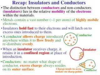
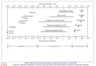
Figure 2.1. Typical range of conductivities for insulators, semiconductors, and conductors. El. Z. Gr. Core . 2. 2. C. 6. IV. 2s. 2p. 2. 2. Si. 14. IV. 3s. 3p. 2. 2. Ge. 32 . IV. 4s. 4p. El. Z. Gr. Core . El. Z. Gr. Core . 2. 1. 2. 3. B. 5. III. 2s.

E N D
Figure 2.1. Typical range of conductivities for insulators, semiconductors, and conductors.
El. Z Gr. Core 2 2 C 6 IV 2s 2p 2 2 Si 14 IV 3s 3p 2 2 Ge 32 IV 4s 4p El. Z Gr. Core El. Z Gr. Core 2 1 2 3 B 5 III 2s 2p N 7 V 2s 2p 2 1 2 3 Al 13 III 3s 3p P 15 V 3s 3p 2 1 2 3 Ga 31 III 4s 4p As 33 V 4s 4p 2 1 2 3 In 49 III 5s 5p Sb 51 V 5s 5p Composti III - V: GaA s, GaP, InSb, InP, GaN, BN, ….. El. Z Gr. Core El. Z Gr. Core 2 2 4 Cd 48 II 5s Te 52 VI 5s 5p Zn C: costante reticolare 0.356 nm Si: costante reticolare 0.543 nm Ge: costante reticolare 0.565 nm 2 2 4 30 II 4s Se 34 VI 4s 4p Composti II - VI: CdTe, CdSe, ZnTe, ….. GaAs: costante reticolare 0.56533 nm AlAs: costante reticolare 0.56605 nm Miscele solide o composti ternari: Ga Al As, In Ga As x 1 - x x 1 - x Composti quaternari: Ga In As P x 1 - x y 1 - y Applicazioni in optoelettronica ed elettronica veloce
IBRIDIZZAZIONE DEGLI ORBITALI ATOMICI Sp3: simmetria tetraedrica Esempio: Carbonio ORBITALI ATOMICI Esempio: Carbonio-atomo isolato
Diamond lattice Zincblende lattice COORDINATE DEI NODI IN UNA CELLA DI DIAMANTE (0,0,0) (0,1,0) (1,0,0) (0,0,1) (1,1,0) (1,0,1) (0,1,1) (1,1,1) (½, ½,0) (½,0 ½) (0, ½, ½) (½, ½,1) (½,1, ½) (1, ½, ½) (1/4,1/4,1/4) (3/4,3/4,1/4) (3/4,1/4,3/4) (1/4,3/4,3/4) 8 NODI PROPRIAMENTE CONTENUTI IN UNA CELLA
Figure 2.11. (a) A tetrahedron bond. (b) Schematic two-dimensional representation of a tetrahedron bond. Legame tetraedrico Rappresentazione bidimensionale di un legame tetraedrico
Figure 2.3. Three cubic-crystal unit cells. (a) Simple cubic (only Po). (b) Body-centered cubic (e.g. Na, W). (c) Face-centered cubic (e.g. Al, Cu, Au, Pt). Figure 2.2. A generalized primitive unit cell.
Trovare le intercette in termini di numeri interi di piani reticolari Prendere i reciproci e ridurli ai più piccoli dei tre interi aventi lo stesso rapporto Miller index per un singolo piano (hkl) Per piani di equivalente simmetria [hkl] Figure 2.5. A (623)-crystal plane. Figure 2.6. Miller indices of some important planes in a cubic crystal.
Densità del silicio = 2.33 g/cm3 Massa atomica = 28.09 g Densità atomica del silicio = 5·1022 atomi/cm3 Costante reticolare del silicio = 0.543 nm Distanza fra primi vicini nel silicio = 0.235 nm Densità superficiale di atomi nel silicio nei piani (100) : 6.78 atomi/nm2 (110) : 9.59 atomi/nm2
Figure 2.14. Schematic representation of an isolated silicon atom.
Figure 2.13. The splitting of a degenerate state into a band of allowed energies.
Figure 2.15. Formation of energy bands as a diamond lattice crystal is formed by bringing isolated silicon atoms together.
Figure 2.16. The parabolic energy (E) vs. momentum (p) curve for a free electron. Figure 2.17.A schematic energy-momentum diagram for a special semiconductor with mn = 0.25 m0 and mp = m0.
Figure 2.18. Energy band structures of Si and GaAs. Circles (º) indicate holes in the valence bands and dots (•) indicate electrons in the conduction bands (GaAs m*=0.063 m; Si m*=0.19 m). Silicon Eg = 1.12 eV GaAs Eg = 1.42 eV
Figure 2.19. Schematic energy band representations of (a) a conductor with two possibilities (either the partially filled conduction band shown at the upper portion or the overlapping bands shown at the lower portion), (b) a semiconductor, and (c) an insulator.
Figure 2.1. Typical range of conductivities for insulators, semiconductors, and conductors.
Figure 2.12. The basic bond representation of intrinsic silicon. (a) A broken bond at Position A, resulting in a conduction electron and a hole. (b) A broken bond at position B.
Fonte: Dispense del corso di Dispositivi Elettronici, Prof. Carlo Naldi, Ed. CELID, 1996
Fonte: Dispense del corso di Dispositivi Elettronici, Prof. Carlo Naldi, Ed. CELID, 1996