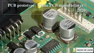
High Temperature PCB Manufacturer
0 likes | 6 Views
Leading high-temperature PCB manufacturer specializing in durable, heat-resistant circuit boards for extreme environments. We offer advanced materials, precise engineering, and reliable performance for aerospace, automotive, and industrial applications.

High Temperature PCB Manufacturer
E N D
Presentation Transcript
WELCOME TO EFPCB.COM
Semiconductor Test Boards: Ensuring Quality in Chip Testing The semiconductor producing area comprises of four essential cycles: semiconductor plan, wafer handling, wafer bundling, and semiconductor testing. The testing system is separated into four classifications: wafer testing, end result testing, framework level testing, and consume in testing. Test cards, load sheets, and consume in sheets (Napkin) are a portion of the PCBs utilized with semiconductor test board. It is a tailor-made item, and the related PCB should be uniquely crafted to match the chip's plan for testing.Read our full blog CLICK.
HDI Printed Circuits: Enabling Advanced Electronics with Higher Performance HDI PCBs are the best of the best in the PCB world, portrayed by their high thickness of parts and guide designs. This is accomplished utilizing better lines and spaces, more modest vias and catch cushions, and higher association cushion densities than found in customary PCBs. The quintessence of HDI innovation lies in its capacity to pack greater usefulness into a more modest space, making it an ideal counterpart for the smaller and complex plans requested by wearable hardware.Check more information about our product CLICK.
HDI PCBs: Driving Innovation in High-Density Electronics HDI PCBs are a wonder of present day gadgets designing, described by their capacity to help a bigger number of associations in a fundamentally more modest space. Dissimilar to conventional PCBs, HDI boards use better lines, more modest vias (openings), and higher association cushion densities. This smallness is critical for current gadgets that request little sizes without compromising execution or usefulness. Read our full blog for more CLICK.
An Overview of Gold Finger PCB Applications The name gold finger literally originated from the material of the component involved and it means the gold plated areas as contacts or connector points. Gold is among the mediums that have the least corrosion resistance and has the highest conductivity of all mediums. Since gold in its purest form is not very physically hard the metals such as nickel and cobalt that are added to make the finger strong and withstand hard use. Another reason is the application. Get more information check our blog CLICK.
Our Organization Our Milestones